JAJSCO1A November   2016  – September 2021 TPS3851

PRODUCTION DATA  

  1. 特長
  2. アプリケーション
  3. 概要
  4. Revision History
  5. Pin Configuration and Functions
  6. Specifications
    1. 6.1 Absolute Maximum Ratings
    2. 6.2 ESD Ratings
    3. 6.3 Recommended Operating Conditions
    4. 6.4 Thermal Information
    5. 6.5 Electrical Characteristics
    6. 6.6 Timing Requirements
    7. 6.7 Timing Diagrams
    8. 6.8 Typical Characteristics
  7. Detailed Description
    1. 7.1 Overview
    2. 7.2 Functional Block Diagram
    3. 7.3 Feature Description
      1. 7.3.1 RESET
      2. 7.3.2 Manual Reset MR
      3. 7.3.3 UV Fault Detection
      4. 7.3.4 Watchdog Mode
        1. 7.3.4.1 CWD
        2. 7.3.4.2 Watchdog Input WDI
        3. 7.3.4.3 Watchdog Output WDO
        4. 7.3.4.4 SET1
    4. 7.4 Device Functional Modes
      1. 7.4.1 VDD is Below VPOR ( VDD < VPOR)
      2. 7.4.2 Above Power-On-Reset, But Less Than VDD(min) (VPOR ≤ VDD < VDD(min))
      3. 7.4.3 Normal Operation (VDD ≥ VDD(min))
  8. Application and Implementation
    1. 8.1 Application Information
      1. 8.1.1 CWD Functionality
        1. 8.1.1.1 Factory-Programmed Timing Options
        2. 8.1.1.2 Adjustable Capacitor Timing
      2. 8.1.2 Overdrive Voltage
    2. 8.2 Typical Application
      1. 8.2.1 Design Requirements
      2. 8.2.2 Detailed Design Procedure
        1. 8.2.2.1 Monitoring the 1.8-V Rail
        2. 8.2.2.2 Calculating RESET and WDO Pullup Resistor
        3. 8.2.2.3 Setting the Watchdog
        4. 8.2.2.4 Watchdog Disabled During Initialization Period
      3. 8.2.3 Glitch Immunity
      4. 8.2.4 Application Curves
  9. Power Supply Recommendations
  10. 10Layout
    1. 10.1 Layout Guidelines
    2. 10.2 Layout Example
  11. 11Device and Documentation Support
    1. 11.1 Device Support
      1. 11.1.1 Device Nomenclature
    2. 11.2 Documentation Support
      1. 11.2.1 Related Documentation
    3. 11.3 Receiving Notification of Documentation Updates
    4. 11.4 サポート・リソース
    5. 11.5 Trademarks
    6. 11.6 Electrostatic Discharge Caution
    7. 11.7 Glossary
  12. 12Mechanical, Packaging, and Orderable Information

パッケージ・オプション

メカニカル・データ(パッケージ|ピン)
サーマルパッド・メカニカル・データ
発注情報

SET1

The SET1 pin can enable and disable the watchdog timer. If SET1 is set to GND, the watchdog timer is disabled and WDI is ignored. If the watchdog timer is disabled, drive the WDI pin to either GND or VDD to ensure that there is no increase in IDD. When SET1 is logic high, the watchdog operates normally. The SET1 pin can be changed dynamically; however, if the watchdog is going from disabled to enabled there is a 150-µs setup time where the watchdog does not respond to changes on WDI, as shown in Figure 7-3.
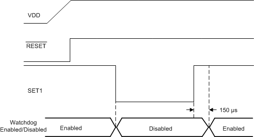
GUID-ACBF3621-5A3E-4F52-8B1E-8A62ACAEC6F4-low.gif Figure 7-3 Enabling and Disabling the Watchdog