SLVS753C February 2007 – November 2016 TPS40180
PRODUCTION DATA.
- 1 Features
- 2 Applications
- 3 Description
- 4 Revision History
- 5 Pin Configuration and Functions
- 6 Specifications
-
7 Detailed Description
- 7.1 Overview
- 7.2 Functional Block Diagram
- 7.3
Feature Description
- 7.3.1 Current Sensing and Overcurrent Detection
- 7.3.2 Hiccup Fault Recovery
- 7.3.3 Selecting Current Sense Network Components
- 7.3.4 PGOOD Functionality
- 7.3.5 Output Overvoltage and Undervoltage Protection
- 7.3.6 Overtemperature Protection
- 7.3.7 eTRIM™
- 7.3.8 Connections Between Controllers for Stacking
- 7.3.9 VSH Line in the Multiphase
- 7.4 Device Functional Modes
- 7.5 Programming
-
8 Application and Implementation
- 8.1 Application Information
- 8.2
Typical Applications
- 8.2.1
Single Output Synchronous Buck Converter
- 8.2.1.1 Design Requirements
- 8.2.1.2
Detailed Design Procedure
- 8.2.1.2.1 Inductor Selection
- 8.2.1.2.2 Output Capacitor Selection
- 8.2.1.2.3 Input Capacitor Selection
- 8.2.1.2.4 MOSFET Selection
- 8.2.1.2.5
Peripheral Component Design
- 8.2.1.2.5.1 Switching Frequency Setting (RT)
- 8.2.1.2.5.2 Output Voltage Setting (FB)
- 8.2.1.2.5.3 Current Sensing Network Design (CS+, CS-)
- 8.2.1.2.5.4 Overcurrent Protection (ILIM)
- 8.2.1.2.5.5 VREG (PVCC)
- 8.2.1.2.5.6 BP5
- 8.2.1.2.5.7 Phase Select (PSEL)
- 8.2.1.2.5.8 VSHARE (VSH)
- 8.2.1.2.5.9 Powergood (PGOOD)
- 8.2.1.2.5.10 Undervoltage Lockout (UVLO)
- 8.2.1.2.5.11 Clock Synchronization (CLKIO)
- 8.2.1.2.5.12 Bootstrap Capacitor
- 8.2.1.2.5.13 Soft Start (SS)
- 8.2.1.2.5.14 Remote Sense
- 8.2.1.2.5.15 Feedback Compensator Design
- 8.2.1.3 Application Curves
- 8.2.2 Simultaneous Tracking With TPS40180 Devices
- 8.2.3 2-Phase Single Output With TPS40180
- 8.2.1
Single Output Synchronous Buck Converter
- 9 Power Supply Recommendations
- 10Layout
- 11Device and Documentation Support
- 12Mechanical, Packaging, and Orderable Information
パッケージ・オプション
メカニカル・データ(パッケージ|ピン)
- RGE|24
サーマルパッド・メカニカル・データ
- RGE|24
発注情報
7 Detailed Description
7.1 Overview
The TPS40180 is a versatile single-phase controller that can be used as a building block for a more complex power system, or as a stand-alone power supply controller. In either system, the TPS40180 provides an excellent power conversion solution and supports such features as prebias start-up, intelligent fault handling capability with graceful shutdown and restart even with multiple modules sharing a common load. Remote load voltage sense for improved load regulation where it counts, at the load, thermal shutdown, remote enable and power good indication features help solve the problems faced by the power supply designer. To ease application to a specific task, there are several user programmable features including closed loop soft-start time, operating frequency and current limit level.
More complex power solutions are readily supported by the TPS40180. The device can be configured to run in a master/slave configuration where a master can control several slaves. Several options are possible including a single output multiple phase supply sharing phase timing information to reduce input and output ripple, a multiple output supply that shares phase switching timing information to reduce input ripple currents, and a combination approach that has multiple outputs sharing phase information where each output can use multiple phases. Phase information in all cases comes from a single device designated the clock master. Current sharing information is passed from the device designated voltage loop master for each output to the slaves for that particular output rail by connecting the COMP pin of the master to the COMP pin of the slaves. The clock master is also the voltage loop master in one of the rails of a multiple output supply; whereas, the other rails are controlled by a voltage loop master that is a clock slave to the single clock master device.
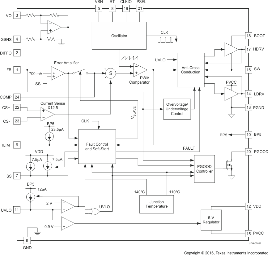
7.2 Functional Block Diagram
7.3 Feature Description
7.3.1 Current Sensing and Overcurrent Detection
The TPS40180 uses the current sensing architecture shown in Figure 20.
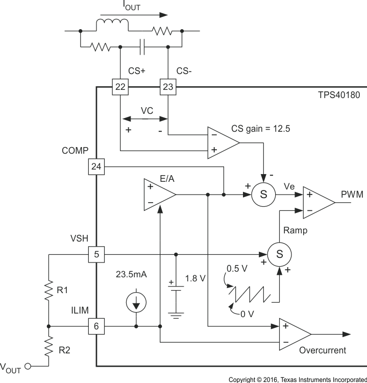 Figure 20. Current Sense Architecture
The sense resistor can either be a resistor between the inductor and the output capacitor(s) or an R-C filter across the inductor.
Overcurrent protection for the TPS40180 is set by connecting a resistor from the ILIM pin to the VSH pin. A current source of 23.5 µA out of the ILIM pin sets a voltage level on the ILIM pin and the COMP pin is not allowed to rise above this level. Since the device uses current mode control and COMP cannot rise above this level, an effective maximum output current is defined. The second resistor on the ILIM pin, R2, is optional and if used is connected to the output voltage. This resistor provides compensation of the overcurrent level for changes in output voltage, such as would be seen at start-up. If not used, the overcurrent threshold level is higher at output voltages lower than the designed target.
The output current, flows through the inductor resistance and develops a voltage, VC across it, representative of the output current. This resistance voltage is extracted from the total inductor voltage by the R-C network placed across the inductor. This voltage is amplified with a gain of 12.5 and then subtracted from the error amplifier output, COMP, to generate the Ve voltage. The Ve signal is compared to the slope-compensation RAMP signal to generate the PWM signal that is used to control the FET drivers. As the output current is increased, the amplified VC causes the Ve signal to decrease. In order to maintain the proper duty cycle, the COMP signal must increase. Therefore, the magnitude of the COMP signal contains the output current information as shown in Equation 1 through Equation 3.


In order to satisfy the input-output voltage relationship, Equation 4 must hold.

Combining Equation 1 and Equation 4 and solving for the COMP voltage gives Equation 5.

Since COMP and ILIM are of equal voltage when at the current limit condition, setting ILIM to the expected COMP voltage at maximum current is how the current limit threshold is set. To calculate the resistors R1 and R2 from Figure 20, use Equation 6 through Equation 9.


where
- COMP is the voltage on the COMP pin
- VRMP is the ramp amplitude, 500 mV
- VOUT is the output voltage of the converter
- IOUT is the dc output current of the converter
- VIN is the input voltage of the converter
- VVSH is the valley voltage of the ramp, 1.8 V
- IPK is the peak current in the inductor
- RL is the DC resistance of the inductor
- L is the inductance of the inductor
- 12.5 is the gain of the current sense amplifier network inside the device
- Nph is the number of phase that the master clock is set to, either 6 or 8
- IILIM is the bias current out of the ILIM pin, 23.5 µA typical
The TPS40180 architecture inherently allows multiple modules to start simultaneously into a load without problems with overcurrent tripping. The reason this is the case is the master device in a group of devices configured as a multiphase power supply is the only device that retains overcurrent control. The slave devices do not have the ability to initiate an overcurrent event but rely on the master to handle this function. For this reason, when setting the overcurrent threshold for a multiple converter system, the previous equations should be used to set the threshold on a per-converter basis. For example, if four converters are being used to generate a supply that has a 60-A current limit, the current limit to use for calculating the resistors would be 15 A.
NOTE
The above equations indicate that the overcurrent threshold is dependent on input voltage. Consequently, as the input voltage increases, the overcurrent threshold also rises.
7.3.2 Hiccup Fault Recovery
To reduce the input current and component dissipation during on overcurrent event, a hiccup mode is implemented. Hiccup mode refers to a sequence of 7 soft-start cycles where no MOSFET switching occurs, and then a re-start is attempted. If the fault has cleared, the re-start results in returning to normal operation and regulation. This is shown in Figure 21.
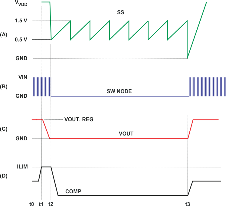 Figure 21. Hiccup Recovery From Faults
Normal operation is occurring between t0 and t1 as shown by VOUT at the regulated voltage, (C) and normal switching on the SW NODE (B) and COMP at its nominal level, (D). At t1, an overcurrent load is experienced. The increased current forces COMP to increase to the ILIM level as shown in (D). If the COMP voltage is above the ILIM voltage for 7 switching cycles, the controller enters a hiccup mode at t2. During this time the controller is not switching and the power MOSFETs are turned off. The SS pin goes through 7 cycles of charging and discharging the soft-start capacitor. At the end of the 7 cycles the controller attempts another normal re-start. If the fault has been cleared, the output voltage comes up to the regulation level as shown at time t3. If the fault has not cleared, the COMP voltage again rises above the ILIM voltage and a fresh hiccup cycle starts. This condition may continue indefinitely.
The prebias circuitry is reset at this time and the restart does not discharge an output prebias condition if it exists.
7.3.3 Selecting Current Sense Network Components
Some consideration must be given to selecting the components that are used to sense current in the converter. If an R-C filter across the inductor is used, the R-C time constant should match the natural time constant of the inductor. Equation 10 and Figure 22 describe the relationship.

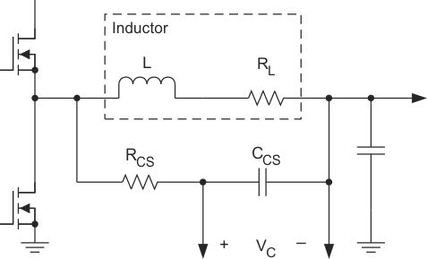 Figure 22. Current Sense Network
The amplitude of the VC voltage must also be considered. If the VC voltage is expected to rise above 60 mV at the desired overcurrent threshold, an attenuator should be used to keep the voltage to a maximum of 60 mV. To implement the divider, place a resistor in parallel with CCS. The time constant of the whole network should remain the same as the L/R time constant of the inductor.
High-ripple current applications can also cause problems under certain conditions. When the sensing network is matched to the inductor, the ripple voltage on the capacitor CCS is the same as the ripple voltage produced on the effective inductor resistance. If this ripple component is too great, subharmonic instability can result and the PWM exhibits excessive jitter or give a long pulse, short pulse type of output. To minimize this effect, the slope of the signal presented to the current sense amplifier must be less than a maximum value. This places a minimum limit on what the inductor L/R time constant can be for a given application as shown in Equation 11. If the chosen inductor and other application parameters fall outside these recommendations, it is necessary to attenuate the current feedback signal with an extra resistor.

where
- L is the inductance in H
- RL is the equivalent series resistance of the inductor in Ω
- GCS(max) is the maximum gain of the current sense amplifier, 13.75
- VIN is the input voltage in V
- VOUT is the output voltage in V
- fSW is the switching frequency in Hz
7.3.4 PGOOD Functionality
PGOOD functions as a normal, open-drain power good output on an device configured as a master. This is an open-drain signal and pulls low when any condition exists that would indicate that the output of the supply might be out of regulation. These conditions include:
- FB pin more that ±15% from nominal
- Soft start is active
- A UVLO condition exists for the TPS40180
- The TPS40180 has detected a short-circuit condition
- The TPS40180 die is over warning temperature threshold (115°C)
If the device is configured as a voltage loop slave, PGOOD pulls low the following conditions only:
- A UVLO condition exists for the TPS40180
- The TPS40180 die is over warning temperature threshold (115°C)
Note that when there is no power to the device, PGOOD is not able to pull close to GND if an auxiliary supply is used for the power good indication.
7.3.5 Output Overvoltage and Undervoltage Protection
If the output voltage is sensed to be too low, the TPS40180 turns off the power FETs, and initiates a hiccup restart sequence just as if a fault condition had occurred. The sensing of the output voltage is done using the FB pin and the undervoltage threshold voltage for the FB pin is 580-mV typical. The prebias circuitry is reset at this time and the restart does not discharge an output prebias condition if it exists.
The TPS40180 also includes an output overvoltage protection mechanism. This mechanism is designed to turn on the low-side FET when the FB pin voltages exceeds the overvoltage protection threshold of 810-mV (typical). The high-side FET turns off and the low-side FET turns on and stays on until the voltage on the FB drops below the undervoltage threshold. At this point, the controller enters a hiccup recovery cycle as in the undervoltage case. The output overvoltage protection scheme is active at all times. If at any time when the controller is enabled, the FB pin voltage exceeds the overvoltage threshold, the low-side FET turns on until the FB pin voltage falls below the undervoltage threshold.
7.3.6 Overtemperature Protection
When the TPS40180 die temperature exceeds 115°C, the PG pin is pulled low as a warning that temperatures are becoming excessive. Systems can act on this indication as appropriate.
The TPS40180 shuts down if the die temperature is sensed to be more than 135°C. The die must cool to less than the warning level reset of 105°C before the device restarts. The device restarts automatically after the die cools to this level.
7.3.7 eTRIM™
The TPS40180 incorporates an innovative new feature that allows the user to trim the reference voltage in system. This allows the user to tighten overall output tolerances by trimming out errors caused by resistor divider and other system tolerances. The reference has been designed so that it may be trimmed without affecting temperature drift so that the user can perform system level trims without worrying about creating a situation where the reference temperature drift becomes a problem. Trimming in the TPS40180 is done with a small bank of EEPROM. Changing bit values in this EEPROM causes parameters, like reference voltage, inside the device to change. Once trim is accomplished, there is no need to trim again, the change is permanent (but can be overwritten by subsequent trimming operations). The eTrim™ trimming mechanism has been designed so that the user can only program the reference voltage so that any errors in the programming sequence does not affect other factory set trims such as current feedback gain for example. This provides a secure environment for the user to use and eliminates the possibility that other parameters could inadvertently changed.
The adjustment range is ±14 mV from the untrimmed level. The reference is pre-trimmed at the factory to ±0.5% of nominal so further trim is not necessary unless it is desired to further reduce total system errors. This factory trim uses the same eTrim™ mechanism that can be used at the system or converter level and changes the same bits that the user changes if using eTrim™. Consequently, not all of the trim range may be available to make adjustments in system as the factory trim sets the bits to the value that provides the correct nominal reference voltage. Typically, the trim has at least 3 steps remaining in any direction to allow for user system level trim.
There are several steps required to use the eTrim™ feature. A typical trim sequence would flow as follows:
- Power up the system and wait for the system to stabilize in steady state
- Program the TPS40180 reference trim to a default setting (overwriting factory trim)
- Measure the system output voltage
- Calculate a correction factor to be applied to the output voltage
- Program the EEPROM inside the TPS40180 with the new trim code
- Measure the new system output voltage
- Repeat from step 4 if required
The TPS40180 provides 4 trim bits available for user programming. The bits and their effect on the untrimmed reference value are given in Table 1.
Table 1. eTrim Bit Codes and Effect
| eTrim™ REFERENCE BIT CODE | REFERENCE CHANGE (mV) | |||
|---|---|---|---|---|
| b3 | b2 | b1 | b0 | |
| 1 | 0 | 0 | 0 | +14 |
| 1 | 0 | 0 | 1 | +12 |
| 1 | 0 | 1 | 0 | +10 |
| 1 | 0 | 1 | 1 | +8 |
| 1 | 1 | 0 | 0 | +6 |
| 1 | 1 | 0 | 1 | +4 |
| 1 | 1 | 1 | 0 | +2 |
| 1 | 1 | 1 | 1 | 0(1) |
| 0 | 0 | 0 | 0 | 0 |
| 0 | 0 | 0 | 1 | –2 |
| 0 | 0 | 1 | 0 | –4 |
| 0 | 0 | 1 | 1 | –6 |
| 0 | 1 | 0 | 0 | –8 |
| 0 | 1 | 0 | 1 | –10 |
| 0 | 1 | 1 | 0 | –12 |
| 0 | 1 | 1 | 1 | –14 |
The process of writing to the on chip trim EEPROM is as follows. With power applied to the system and the system in steady state:
- Force the input voltage to the device, VVDD, to a level of 7 V (this eases stresses on the UVLO pin).
- Raise the UVLO pin to a level 2 V above VVDD and PGOOD to 20 V
- Apply a pulse of VVDD + 4 V for a minimum of 10 µs to UVLO
- Bring UVLO to VVDD + 2 V for at least 8 µs
- The UVLO pin is then pulsed to VVDD + 4 V seven times (six address bits and one data bit) for each bit that is to be written. The pulse period is typically 1 µs and the width of the pulse determines whether the pulse is interpreted as a 1 or as a 0 by the EEPROM circuitry.
- Data has been placed in a buffer. To finalize the writing, pull PGOOD to 20 V and the UVLO pin to
VVDD + 4 V for at least 15 ms.
Figure 23 shows a typical sequence.
 Figure 23. eTrim™ EEPROM Programming Sequence
The pulses from VVDD + 2 V to VVDD + 4 V on UVLO are governed by the timing shown in Figure 24.
There are six address bits in the sequence to write to a single EEPROM bit. To write to the eTrim™ accessible bits, the address sequence must be correct for all six bits or else the write attempt has no effect. To write to eTrim™ accessible bits the first four address bits must be zero. Anything else is not accepted. Address bits A1 and A0 select which eTrim™ accessible EEPROM bit is written. For example, to write a 1 to bit 3 of the eTrim™ accessible bits, the data pulse sequence would look like Figure 25.
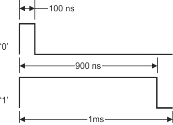 Figure 24. eTrim™ Bit Pulse Timing
 Figure 25. Write 1 to Bit 3
As data is clocked into the device, the reference voltage reflects the updates without writing the data buffer to the actual EEPROM. System measurements can be made after a suitable system dependent settling time has elapsed after changing the bits in the buffer. When satisfied with the results, the EEPROM may be written by pulling PGOOD to 20 V and UVLO to VVDD + 4 V for at least 15 ms. For best reliability, the EEPROM should only be written to by pulling PGOOD to 20 V and UVLO to VVDD + 4 V a maximum of three times during the product lifetime. This writing only needs to be done once during the entire trimming cycle, after the optimal trim values are found since data clocked in will affect the output without performing the actual write. Until written, changes are not permanent and will be lost after power cycling the device.
7.3.8 Connections Between Controllers for Stacking
One of the main benefits of using the TPS40180 is the ability to parallel output power stages to achieve higher output currents and to scale or stack on controllers as needed. Phasing information is also shared among the controllers to minimize input ripple and RMS current in the input stage capacitors. Figure 26 shows the connections among the controller devices and the controller configuration connections to implement a single output stacked configuration. Up to 7 slave controllers can be connected to the master controller in this manner with unique phasing for each controller. More than 7 controllers can also be connected as long as some of them are programmed to operate at the same phase relationship with respect to the master. Not shown are the power stage portions of the schematics. The outputs of the individual converters inductors are simply connected together and then to a common output capacitor bank. All other connections would be as for a single device used as a converter.
In Figure 26, the master controller is configured as a CLK master and as a voltage control loop master (SS and RT pin connections). The slave controllers are configured as CLK slaves (RT pin tied to PVCC) and as voltage control loop slaves (SS pin tied to PVCC).
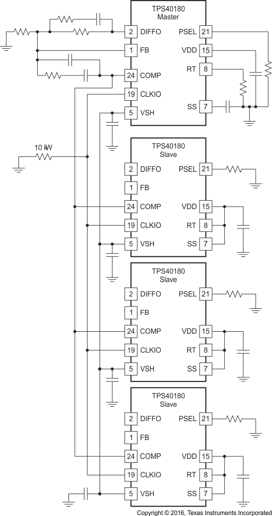 Figure 26. Single-Output Stacked Configuration
The 10-kΩ resistor connected from the CLKIO line to GND is required to ensure that the CLKIO line falls to GND quickly when the master device is shutdown or powers off. The master CLKIO pin goes to a high impedance state at these times and if the CLKIO line was high, there is no other active discharge part. The slave controllers look at the CLKIO line to determine if the system is supposed to be running or not. A level below 0.5 V on CLKIO is required for this purpose. If the CLKIO line remains high after that master is shut down, the slaves continue to operate. This is seen as the slave LDRV signal remaining high for a period of time after the master is shut down and results in output voltage excursions that are not controlled.
NOTE
In any system configured to have a CLK master and CLK slaves, a 10-kΩ resistor connected from CLKIO to GND is required.
For simplicity of design, the compensation components shown on the master, as well as the components connected to the RT and SS pins may be present on the slaves. This prevents separate designs being necessary for master and slave circuits. The RT and SS pins can have jumper option to tie them to VDD to program an individual device as a slave. These components were omitted in Figure 26.
Selection of the PSEL pin resistors is simple. First determine if the master should generate a CLK signal that is suitable for 60 or 45 spacing of the phases. Select the appropriate PSEL connection option from Table 3. For the slaves, determine the desired firing angle for each one and pick the appropriate resistor from either Table 4 or Table 5 depending on the clock scheme chosen for the master.
Design Note: When used in a master/slave relationship and an overvoltage event occurs, only the control loop master turns on the low-side FET to pull down the output voltage. This results in the master phase low-side FET sinking all of the combined maximum current for the slaves. For example, if the per phase current limit is 10 A and there are 4 phases, the master low-side FET could be required to pass 30 A for a brief time. The master error amplifier is still active during this time and tries to have the slaves regulate the output voltage. As the master COMP pin rises to the ILIM point, a fault event is sensed and the converter shuts down, and then initiate a hiccup restart. Size the master low-side FET to handle the appropriate amount of surge current for 7 clock cycles of the converter.
A connection diagram for several controllers sharing phase information and synchronized to each other but having different output voltages is shown in Figure 27. This is similar to the previous example but here the controllers are all control loop masters (SS not pulled to VDD) and control their own output voltages independently. One device is configured as a CLK master (RT not tied to VDD) and is the clock generator for the CLK slaves. Picking the PSEL resistors is the same as before. overcurrent in this configuration depends on which controller senses the overcurrent event. If one of the CLK slaves experiences a fault, that converter only shuts down, and enter the hiccup restart mode. If the CLK master controller senses an overcurrent, it stops sending CLKIO pulses to the slaves, causing them to stop. The master then enters a hiccup recovery mode.
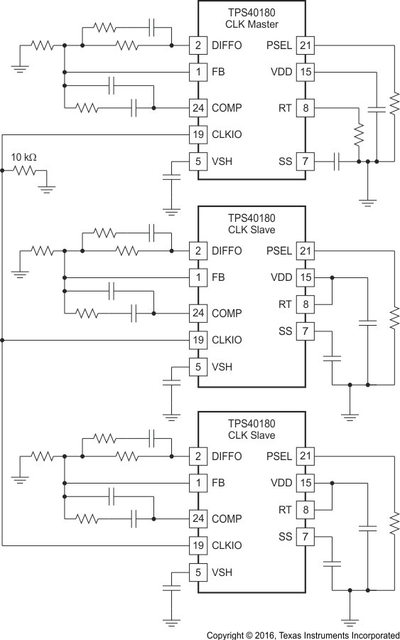 Figure 27. Phase Share Multiple Output Configuration
Finally, a configuration diagram for multiple multiphase converters is shown in Figure 28. This is just a combination of the two previous examples and should follow intuitively once those are understood. It is the example of Figure 26 with a CLK slave but control loop master added to create a second output voltage while sharing phasing information with the first converter group. A slave has been added to the second control loop master controller in this case as well creating a grouping of controllers that provide a second output voltage. This can have a significant impact on the required input filter capacitance if all the converters are located close to one another.
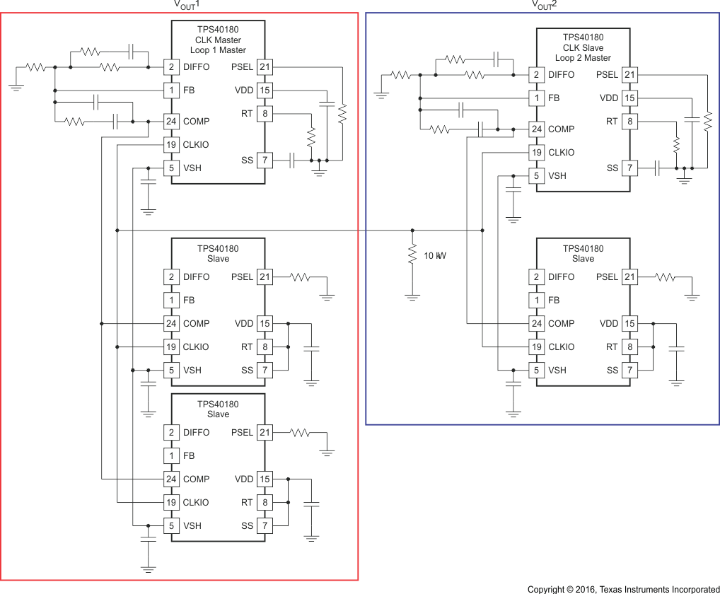 Figure 28. Multiple Multiphase Configuration
7.3.9 VSH Line in the Multiphase
The examples in Figure 26, Figure 27, and Figure 28 show the VSH line distributed among the various controllers comprising a single-output voltage grouping. This is the recommended practice for best results. However, if the ground potential difference between the controllers is not great (no more that 10 mV), distribution of VSH among the controllers in a particular output voltage group may not be necessary. VSH is the valley voltage of the controller and distributing it provides a known current reference signal among the controllers that when compared with the distributed COMP signal from the master, serves to better balance the current among the modules. If the ground potential between modules in the same output voltage grouping is small enough, there error contributed by not distributing the VSH signal becomes on the order of systematic errors already present and its usefulness is diminished. A decision must be made on an individual application basis.
7.4 Device Functional Modes
7.4.1 Tracking
The TPS40180 can function in a tracking mode, where the output tracks some other voltage. To do this, a voltage divider is connected from the voltage to be tracked to GND, with the tap of the divider connected to the SS pin of the TPS40180 (see Figure 29). The capacitors C1 and C2 are required for two purposes. First they provide a means for timing of overcurrent restart attempts. Second, they provide for matching output voltage ramp up rate of the TPS40180 to the controlling external supply.
When choosing component values, the SS pin current (ISS) must be accounted for in order to prevent an offset in the output of the TPS40180 converter and the tracked supply.

where
- R1, R2, R3, and R5 are in Ω
- VREF is the reference voltage fo the TPS40180, 700 mV
- I(SS) is the SS pin current, 15 µA typical
To use Equation 12, R3 and R5 must be known from the design of the compensation network and nominal converter output voltage. R2 is then chosen arbitrarily. A value between 1 kΩ and 10 kΩ is suggested. Too large a value and the tracking error is greater. Too small, and the requirements for C2 and C2 become excessive. Once R1 and R2 have been chosen, C1 and C2 can be chosen. The R1-C1 time constant and the R2 C2 time constant should match as in Equation 13.

Absolute matching of the time constants is not necessary for Equation 13. The nearest standard values of capacitor provides satisfactory results. Pick a value for C1 or C2 and find the closest corresponding standard value for the other capacitor.
7.5 Programming
7.5.1 Programming the Operating Frequency
A resistor is connected from the RT pin to GND to select the operating frequency of the converter. The relationship between the desired operating frequency and the timing resistance is given by Equation 14.

where
- RRT is the timing resistance in kΩ
- fSW is the desired switching frequency in kHz
If this is a clock master, the switching frequency above is the per-phase switching frequency.
7.5.2 Programming the Soft-Start Time
The soft-start time is programmable by connecting a capacitor from the SS pin to GND. An internal current source charges this capacitor providing a linear ramp voltage. This ramp voltage is the effective reference to the error amplifier while it is less that the 700-mV internal reference. The time required for the SS pin to ramp from GND to 700 mV is the soft-start time. For outputs that are not prebiased, that time is given in Equation 15.

where
- tSS is the soft-start time in seconds
- CSS is the capacitor from SS to GND in µF
- ISS is the soft-start current in µA, 15-µA typical
If the output of the converter has a pre-existing voltage on it, the soft start occurs a little differently. The SS pin current is held to a lower value than normal until the PWM becomes active. This occurs as the SS pin voltage exceeds the FB pin voltage and the COMP pin moves up into the ramp range, causing the first pulse. At that point, the SS pin current is shifted to 15 µA nominal. Figure 30 and Figure 31 illustrate this.
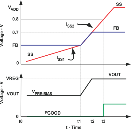 Figure 30. Soft-Start Waveform for Prebiased Outputs
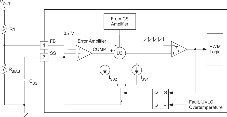 Figure 31. Soft-Start Implementation
Using Figure 30 provides Equation 16, Equation 17, and Equation 18.


where
- t1 is the time to the first PWM pulse in seconds
- t2 is the time from the first PWM pulse until regulation in seconds
- C(SS) is the SS pin capacitor in µF
- I(SS1) is the SS1 pin charging current in µA, 7.5 µA
- I(SS2) is the SS2 pin charging current in µA, 15 µA
- TSS is the total soft-start time
7.5.3 Using the Device for Clock Master/Slave Operation
The TPS40180 can be operated as either a master clock source or a slave to a master clock as seen in Table 2.
Table 2. RT Voltage and Clock Master/Slave
| RT VOLTAGE (VRT) | CLOCK MODE |
|---|---|
| < 0.5 V | Master (or single converter) |
| > 2 V (tied to PVCC or VDD) | Slave |
In the clock master mode, the master clock frequency is set by connecting a resistor from the RT pin to GND. In the clock master mode, the PSEL pin selects the CLKIO operating mode for the device. There are three possible states defined in Table 3.
Table 3. PSEL Pin Modes for Clock Master
| PSEL RESISTANCE TO GND (kΩ) | MODE |
|---|---|
| 0 | No CLKIO, CLKIO does not send out pulses |
| OPEN | 8 phase CLKIO, CLKIO send out a pulse train for interleaving with 45° phase separation |
| 29.4 | 6 phase CLKIO, CLKIO send out a pulse train for interleaving with 60° phase separation |
In the clock slave mode, the CLKIO pin is an input. The controller fires in a fixed relationship to the master determined by the resistance placed from PSEL to GND, or is turned off to improve efficiency at light load. The actual result depends on how the master CLKIO is programmed in either Table 4 or Table 5.
Table 4. PSEL Phase Programming for Slave With 8 Phase Master Clock
| PHASE ANGLE (°) | PSEL RESISTANCE TO GND (kΩ) |
|---|---|
| Standby | OPEN |
| 45 | 0 |
| 90 | 14.7 |
| 135 | 29.4 |
| 180 | 47 |
| 225 | 68 |
| 270 | 95.3 |
| 315 | 127 |
Table 5. PSEL Phase Programming for Slave With 6 Phase Master Clock
| PHASE ANGLE (°) | PSEL RESISTANCE TO GND (kΩ) |
|---|---|
| Standby | OPEN |
| 0 | 95.3 |
| 60 | 0 |
| 120 | 14.7 |
| 180 | 29.4 |
| 240 | 47 |
| 300 | 68 |
When a slave senses any level change on the PSEL pin that would indicate a change in firing angle, it momentarily goes into standby mode. When a slave leaves standby mode, it starts supplying current after 64 clock cycles have elapsed if the status of the PSEL pin has not changed from when the device entered standby mode. In this way, a slave can have its firing angle dynamically changed depending on operating conditions. A slave can be held in standby mode by allowing the PSEL pin to float.
7.5.4 Using the TPS40180 for Voltage Control Loop Master or Slave Operation
The TPS40180 can function as a voltage loop master or as a voltage loop slave. As a voltage loop master, the TPS40180 behaves like a standard control device in that it regulates its output using its internal error amplifier and reference. As a voltage loop slave, the TPS40180 takes the VSH and COMP signals from a voltage loop master and the slave converter becomes an output current booster to the master converter. Current is shared between the master and slave since both the current command reference (VSH) and the current command (COMP) are being distributed form the master controller and used by the slave to set its output current. The error amplifier in the master is responsible for overall voltage regulation. The error amplifier on the slave is disconnected when configured as a voltage control loop slave.
To configure a TPS40180 as a voltage loop slave, connect the SS pin to VDD or PVCC. It is important that the SS pin not fall more than 1 V below the PVCC voltage when starting up as a slave. If this condition is no met, the controller may not start. For this reason, it is not recommended to tie SS to BP5 to configure the converter as a voltage control loop slave.