JAJS132D July 2005 – June 2019 TPS40190
PRODUCTION DATA.
- 1 特長
- 2 アプリケーション
- 3 概要
- 4 改訂履歴
- 5 Pin Configuration and Functions
- 6 Specifications
- 7 Detailed Description
- 8 Application and Implementation
- 9 デバイスおよびドキュメントのサポート
- 10メカニカル、パッケージ、および注文情報
パッケージ・オプション
デバイスごとのパッケージ図は、PDF版データシートをご参照ください。
メカニカル・データ(パッケージ|ピン)
- DRC|10
サーマルパッド・メカニカル・データ
- DRC|10
発注情報
7.3.3 Enable Functionality
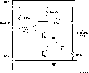
The TPS40190 has a dedicated ENABLE pin. This simplifies user level interface design since no multiplexed functions exist. Another benefit is a true low power shutdown mode of operation. In this state, the BP5 regulator is turned off. When the ENABLE pin is pulled to GND, the TPS40190 consumes a typical 20-μA of current. A functionally equivalent circuit to the enable circuitry on the TPS40190 is shown in Figure 24.
 Figure 24. TPS40190 ENABLE Pin Internal Circuitry
 If the ENABLE pin is left floating, the chip starts automatically. The pin must be pulled to less than 600 mV to ensure that the TPS40190 is in shutdown mode. Note that the ENABLE pin is relatively high impedance. In some situations, there could be enough noise nearby to cause the ENABLE pin to swing below the 600 mV threshold and give erroneous shutdown commands to the rest of the device. There are two solutions to this problem should it arise.
- Place a capacitor from ENABLE to GND. A side effect of this is to delay the start of the converter while the capacitor charges past the enable threshold
- Place a resistor from VDD to ENABLE. This causes more current to flow in the shutdown mode, but does not delay converter startup. If a resistor is used, the total current into the ENABLE pin should be limited to no more than 500 μA.
The ENABLE pin is self-clamping. The clamp voltage can be as low as 1 V with a 1-kΩ ground impedance. Due to this self-clamping feature, the pull-up impedance on the ENABLE pin should be selected to limit the sink current to less than 500 μA. Driving the ENABLE pin with a low-impedance source voltage can result in damage to the device. Because of the self-clamping feature, it requires care when connecting multiple ENABLE pins together. For enabling multiple TPS4019x devices (TPS40190, TPS40192, TPS40193, TPS40195, TPS40197), see the Application Report SLVA509.
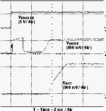
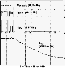
Typical waveforms for startup and shutdown using the ENABLE pin are shown in Figure 25 and Figure 26.
 Figure 25. Startup Using ENABLE Pin
  Figure 26. Shutdown Using ENABLE Pin