SLUS930D April 2011 – November 2016 TPS40400
PRODUCTION DATA.
- 1 Features
- 2 Applications
- 3 Description
- 4 Revision History
- 5 Pin Configuration and Functions
- 6 Specifications
-
7 Detailed Description
- 7.1 Overview
- 7.2 Functional Block Diagram
- 7.3
Feature Description
- 7.3.1 Output Voltage Setting
- 7.3.2 Input Voltage Feedforward
- 7.3.3 Output Current Limit and Warning
- 7.3.4 Linear Regulators
- 7.3.5 PMBus Address
- 7.3.6 PMBus Connections
- 7.3.7
PMBus Functionality and Additional Set-Up
- 7.3.7.1 Data Format
- 7.3.7.2 Output Voltage Adjustment
- 7.3.7.3 Overcurrent Threshold
- 7.3.7.4 Output Current Reading
- 7.3.7.5 Soft-Start Time
- 7.3.7.6 Power Good
- 7.3.7.7 Undervoltage Lockout (UVLO)
- 7.3.7.8 Output Overvoltage and Undervoltage Thresholds
- 7.3.7.9 Programmable Fault Responses
- 7.3.7.10 User Data and Adjustable Anti-Cross-Conduction Delay
- 7.4 Device Functional Modes
- 7.5 Programming
- 7.6
Register Maps
- 7.6.1 OPERATION (01h)
- 7.6.2 ON_OFF_CONFIG (02h)
- 7.6.3 CLEAR_FAULTS (03h)
- 7.6.4 WRITE_PROTECT (10h)
- 7.6.5 STORE_DEFAULT_ALL (11h)
- 7.6.6 RESTORE_DEFAULT_ALL (12h)
- 7.6.7 STORE_DEFAULT_CODE (13h)
- 7.6.8 RESTORE_DEFAULT_CODE (14h)
- 7.6.9 VOUT_MODE (20h)
- 7.6.10 VOUT_TRIM (22h)
- 7.6.11 VOUT_MARGIN_HIGH (25h)
- 7.6.12 VOUT_MARGIN_LOW (26h)
- 7.6.13 VOUT_SCALE_LOOP (29h)
- 7.6.14 FREQUENCY_SWITCH (33h)
- 7.6.15 VIN_ON (35h)
- 7.6.16 VIN_OFF (36h)
- 7.6.17 IOUT_CAL_GAIN (38h)
- 7.6.18 IOUT_CAL_OFFSET (39h)
- 7.6.19 VOUT_OV_FAULT_LIMIT (40h)
- 7.6.20 VOUT_OV_FAULT_RESPONSE (41h)
- 7.6.21 VOUT_UV_FAULT_LIMIT (44h)
- 7.6.22 VOUT_UV_FAULT_RESPONSE (45h)
- 7.6.23 IOUT_OC_FAULT_LIMIT (46h)
- 7.6.24 IOUT_OC_FAULT_RESPONSE (47h)
- 7.6.25 IOUT_OC_WARN_LIMIT (4Ah)
- 7.6.26 OT_FAULT_RESPONSE (50h)
- 7.6.27 POWER_GOOD_ON (5Eh)
- 7.6.28 POWER_GOOD_OFF (5Fh)
- 7.6.29 TON_RISE (61h)
- 7.6.30 STATUS_BYTE (78h)
- 7.6.31 STATUS_WORD (78h)
- 7.6.32 STATUS_VOUT (7Ah)
- 7.6.33 STATUS_IOUT (7Bh)
- 7.6.34 STATUS_TEMPERATURE (7Dh)
- 7.6.35 STATUS_CML (7Eh)
- 7.6.36 READ_VIN (88h)
- 7.6.37 READ_VOUT (8Bh)
- 7.6.38 READ_IOUT (8Ch)
- 7.6.39 PMBUS_REVISION (98h)
- 7.6.40 MFR_VIN_MIN (A0h)
- 7.6.41 MFR_VIN_MAX (A1h)
- 7.6.42 MFR_VOUT_MIN (A4h)
- 7.6.43 MFR_VOUT_MAX (A5h)
- 7.6.44 MFR_SPECIFIC_00 (D0h)
- 7.6.45 MFR_SPECIFIC_01 (D1h)
- 7.6.46 MFR_SPECIFIC_02 (D2h)
- 7.6.47 MFR_SPECIFIC_03 (D3h)
- 7.6.48 MFR_SPECIFIC_04 (D4h)
- 7.6.49 MFR_SPECIFIC_05 (D5h)
- 7.6.50 MFR_SPECIFIC_06 (D6h)
- 7.6.51 MFR_SPECIFIC_07 (D7h)
- 7.6.52 MFR_SPECIFIC_44 (FCh)
-
8 Application and Implementation
- 8.1 Application Information
- 8.2
Typical Applications
- 8.2.1
TPS40400 12-V Input, 1.2-V Output, 20-A (maximum) Output Current ConverterAdded Design Example 1
- 8.2.1.1 Design Requirements
- 8.2.1.2
Detailed Design Procedure
- 8.2.1.2.1 Selecting a Switching Frequency
- 8.2.1.2.2 Output Inductor, LOUT
- 8.2.1.2.3 Output Capacitance, COUT
- 8.2.1.2.4 The Resistive Component of Output Ripple
- 8.2.1.2.5 Peak Current Rating of the Inductor
- 8.2.1.2.6 Input Capacitance, CIN
- 8.2.1.2.7 Switching MOSFETs, QHS and QLS
- 8.2.1.2.8 Device Addressing, RADDR0 and RADDR1
- 8.2.1.2.9 Current Sense Flter, R16 and C17
- 8.2.1.2.10 Voltage Decoupling Capacitors, CBP3, CBP6, and CVDD
- 8.2.1.2.11 Bootstrap Capacitor, C9
- 8.2.1.2.12 Snubber R12 and C16
- 8.2.1.2.13 Loop Compensaton Components
- 8.2.1.2.14 Output Voltage Set Point, RBIAS
- 8.2.1.2.15 Remote Sensing
- 8.2.1.3 Application Curves
- 8.2.2 TPS40400 12-V Input 5-V Output, 5-A (Maximum) Output Current Converter Design Example 2Added Design Example 2
- 8.2.1
TPS40400 12-V Input, 1.2-V Output, 20-A (maximum) Output Current ConverterAdded Design Example 1
- 8.3 Initialization Setup
- 9 Power Supply Recommendations
- 10Layout
- 11Device and Documentation Support
- 12Mechanical, Packaging, and Orderable Information
1 Features
- Input Operating Voltage Range: 3 V to 20 V
- PMBus Enabled Analog Controller
- Reference 600 mV ± 1%
- Remote Voltage Sense Amplifier
- Internal 6-V Regulator and 6-V Gate Drive
- Programmable Overcurrent Protection
- Inductor Resistance or Series Resistance Used for Current Sensing
- Programmable Switching Frequency: 200 kHz to 2 MHz
- Powergood Indicator
- Thermal Shutdown
- Programmable Soft-Start
- Internal Bootstrap Diode
- Prebias Output Safe
- 24-Pin QFN Package
2 Applications
- Smart Power Systems
- Power Supply Modules
- Communications Equipment
- Computing Equipment
3 Description
The TPS40400 is a cost-optimized flexible synchronous buck controller that operates from a nominal 3-V to 20-V supply. This controller is an analog PWM controller that allows programming and monitoring through the PMBus™ interface. Flexible features found on this device include programmable soft-start time, programmable short circuit limit, and programmable undervoltage lockout (UVLO).
An adaptive anti-cross conduction scheme is used to prevent shoot through current in the power FETs. Gate drive voltage is 6 V to better enhance the power FETs for reduced losses. Short circuit detection occurs by sensing the voltage drop across the inductor or across a resistor placed in series with the inductor. A PMBus programmable threshold is compared to this voltage and is used to detect overcurrent. When the overcurrent threshold is reached, a pulse by pulse current limit scheme is used to limit the current to acceptable levels. If the overcurrent condition persists for more than 7 clock cycles of the converter, a fault condition is declared and the converter shuts down and goes into either a hiccup restart mode or latches off. The behavior can be selected through the PMBus interface. Other PMBus interface features include programmable operating frequency, soft-start time, overvoltage and undervoltage thresholds and the response to those events, output voltage change including margining as well as status monitoring.
- For all available packages, see the orderable addendum at the end of the data sheet.
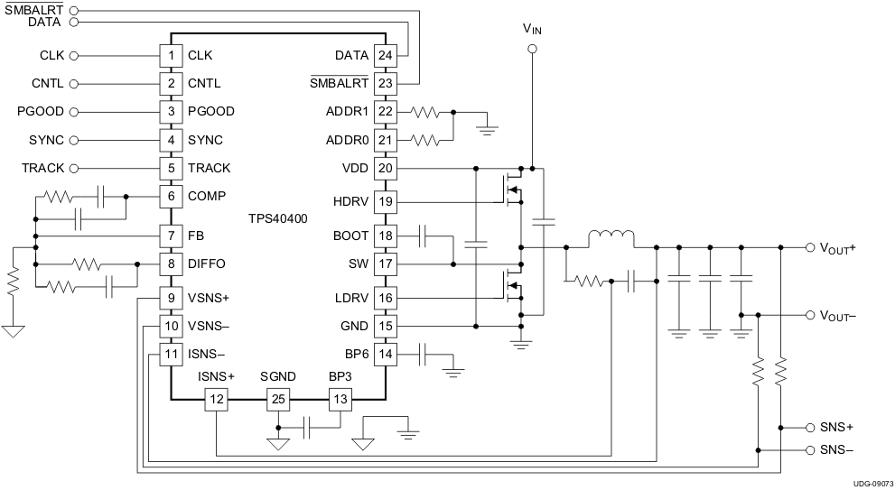
Simplified Application
