SLUS786H OCTOBER 2007 – January 2015 TPS51125
PRODUCTION DATA.
- 1 Features
- 2 Applications
- 3 Description
- 4 Revision History
- 5 Pin Configuration and Functions
- 6 Specifications
-
7 Detailed Description
- 7.1 Overview
- 7.2 Functional Block Diagram
- 7.3
Feature Description
- 7.3.1 PWM Operations
- 7.3.2 Adaptive On-Time Control and PWM Frequency
- 7.3.3 Loop Compensation
- 7.3.4 Ramp Signal
- 7.3.5 Light-Load Condition in Auto-Skip Operation
- 7.3.6 Out-of-Audio Light-Load Operation
- 7.3.7 VREG5/VREG3 Linear Regulators
- 7.3.8 VREG5 Switch Over
- 7.3.9 VREG3 Switch Over
- 7.3.10 Powergood
- 7.3.11 Output Discharge Control
- 7.3.12 Low-Side Driver
- 7.3.13 High-Side Driver
- 7.3.14 VCLK for Charge Pump
- 7.3.15 Current Protection
- 7.3.16 Overvoltage and Undervoltage Protection
- 7.3.17 UVLO Protection
- 7.3.18 Thermal Shutdown
- 7.4 Device Functional Modes
- 8 Application and Implementation
- 9 Power Supply Recommendations
- 10Layout
- 11Device and Documentation Support
- 12Mechanical, Packaging, and Orderable Information
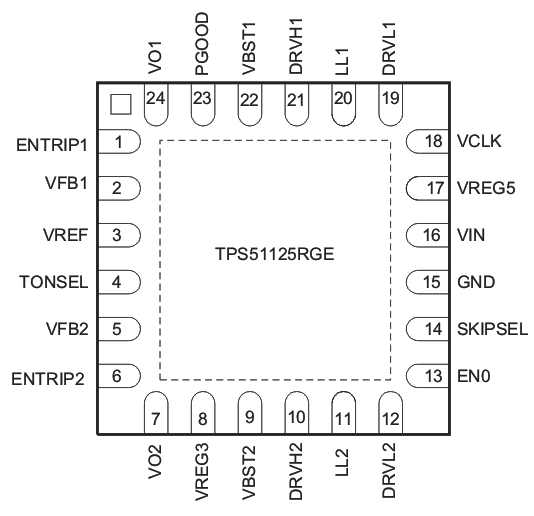
5 Pin Configuration and Functions
RGE PACKAGE
24 PINS
TOP VIEW

Pin Functions
| PIN | I/O | DESCRIPTION | |
|---|---|---|---|
| NAME | NO. | ||
| DRVH1 | 21 | O | High-side N-channel MOSFET driver outputs. LL referenced drivers. |
| DRVH2 | 10 | ||
| DRVL1 | 19 | O | Low-side N-channel MOSFET driver outputs. GND referenced drivers. |
| DRVL2 | 12 | ||
| ENTRIP1 | 1 | I/O | Channel 1 and Channel 2 enable and OCL trip setting pins.Connect resistor from this pin to GND to set threshold for synchronous RDS(on) sense. Short to ground to shutdown a switcher channel. |
| ENTRIP2 | 6 | ||
| EN0 | 13 | I/O |
Master enable input. Open : LDOs on, and ready to turn on VCLK and switcher channels. 620 kΩ to GND : enable both LDOs, VCLK off and ready to turn on switcher channels. Power consumption is almost the same as the case of VCLK = ON. GND : disable all circuit |
| GND | 15 | — | Ground. |
| LL1 | 20 | I | Switch node connections for high-side drivers, current limit and control circuitry. |
| LL2 | 11 | ||
| PGOOD | 23 | O | Power Good window comparator output for channel 1 and 2. (Logical AND) |
| SKIPSEL | 14 | I |
Selection pin for operation mode: OOA auto skip : Connect to VREG3 or VREG5 Auto skip : Connect to VREF Auto skip : Connect to VREF |
| TONSEL | 4 | I |
On-time adjustment pin 365 kHz/460 kHz setting : connect to VREG5 300 kHz/375 kHz setting : connect to VREG3 245 kHz/305 kHz setting : connect to VREF 200 kHz/250 kHz setting : connect to GND |
| VBST1 | 22 | I | Supply input for high-side N-channel MOSFET driver (boost terminal). |
| VBST2 | 9 | ||
| VCLK | 18 | O | 270-kHz clock output for 15-V charge pump. |
| VFB1 | 2 | I | SMPS feedback inputs. Connect with feedback resistor divider. |
| VFB2 | 5 | ||
| VIN | 16 | I | High voltage power supply input for 5-V/3.3-V LDO. |
| VO1 | 24 | I/O | Output connection to SMPS. These terminals work as fixed voltage inputs and output discharge inputs. VO1 and VO2 also work as 5 V and 3.3 V switch over return power input respectively. |
| VO2 | 7 | ||
| VREF | 3 | O | 2-V reference voltage output. Connect 220-nF to 1-μF ceramic capacitor to Signal GND near the device. |
| VREG3 | 8 | O | 3.3-V power supply output. Connect 10-μF ceramic capacitor to Power GND near the device. A 1-μF ceramic capacitor is acceptable when not loaded. |
| VREG5 | 17 | O | 5-V power supply output. Connect 33-μF ceramic capacitor to Power GND near the device. |