SLUSDW9A June 2020 – June 2020 TPS51215A
PRODUCTION DATA.
- 1 Features
- 2 Applications
- 3 Description
- 4 Revision History
- 5 Pin Configuration and Functions
- 6 Specifications
-
7 Detailed Description
- 7.1 Overview
- 7.2 Functional Block Diagram
- 7.3
Feature Description
- 7.3.1 Switch Mode Power Supply Control
- 7.3.2 VREF, V0, V1, V2, V3 and Output Voltage
- 7.3.3 Soft-Start and Power Good
- 7.3.4 SLEW and VID Function
- 7.3.5 MODE Pin Configuration
- 7.3.6 Light-Load Operation
- 7.3.7 Out-of-Bound Operation
- 7.3.8 Current Sensing and Overcurrent Protection
- 7.3.9 Overvoltage and Undervoltage Protection
- 7.3.10 V5IN Undervoltage Lockout Protection
- 7.3.11 Thermal Shutdown
- 7.4 D-CAP2 Control Mode
- 8 Application and Implementation
-
9 Typical Applications
- 9.1 Design Requirements
- 9.2
Detailed Design Procedure
- 9.2.1 Step One: Determine the Specifications
- 9.2.2 Step Two: Determine System Parameters
- 9.2.3 Step Three: Determine Inductor Value and Choose Inductor
- 9.2.4 Step Four: Set the Output Voltages
- 9.2.5 Step Five: Calculate SLEW Capacitance
- 9.2.6 Step Six
- 9.2.7 Step Seven: Determine the Output Capacitance
- 9.2.8 Step Eight: Select Decoupling and Peripheral Components
- 9.3 Application Examples
- 9.4 Application Curves of Design 1
- 10Power Supply Recommendations
- 11Layout
- 12Device and Documentation Support
- 13Mechanical, Packaging, and Orderable Information
パッケージ・オプション
メカニカル・データ(パッケージ|ピン)
- RUK|20
サーマルパッド・メカニカル・データ
- RUK|20
発注情報
7.4 D-CAP2 Control Mode
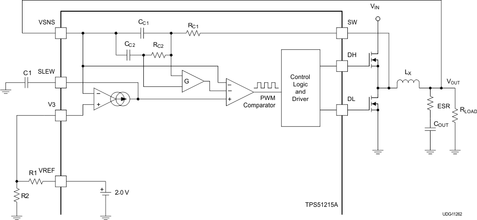
Figure 11 shows a simplified model of D-CAP2 mode architecture in the TPS51215A.
 Figure 11. Simplified D-CAP2 Mode Architecture
 When TPS51215A operates in D-CAP2 mode, it uses an internal phase compensation network (RC1, RC2, CC1 and CC2 and G) to work with very low ESR output capacitors such as multi-layer ceramic capacitors (MLCC) and POSCAP. The role of such network is to sense and scale the ripple component of the inductor current information and then use it in conjunction with the voltage feedback to achieve loop stability of the converter.
The switching frequency used for D-CAP2 mode is 600 kHz and it is generally recommended to have a unity gain crossover (f0) of 1/4 of the switching frequency, which is approximately 150 kHz for the purpose of this application.
Given the range of the recommended unity gain frequency, the power stage design is flexible, as long as Equation 6 is true.

When TPS51215A is configured in D-CAP2 mode, the overall loop response is dominated by the internal phase compensation network. The compensation network is designed to have two identical zeros at 7.7 kHz in the frequency domain, which serves the purpose of splitting the L-C double pole into one low frequency pole (same as the L-C double pole frequency) and one high-frequency pole (greater than the unity gain crossover frequency).