JAJS529A December 2010 – October 2016 TPS53310
PRODUCTION DATA.
- 1 特長
- 2 アプリケーション
- 3 概要
- 4 改訂履歴
- 5 Pin Configuration and Functions
- 6 Specifications
- 7 Detailed Description
- 8 Application and Implementation
- 9 Power Supply Recommendations
- 10Layout
- 11デバイスおよびドキュメントのサポート
- 12メカニカル、パッケージ、および注文情報
パッケージ・オプション
メカニカル・データ(パッケージ|ピン)
- RGT|16
サーマルパッド・メカニカル・データ
- RGT|16
発注情報
8 Application and Implementation
NOTE
Information in the following applications sections is not part of the TI component specification, and TI does not warrant its accuracy or completeness. TI’s customers are responsible for determining suitability of components for their purposes. Customers should validate and test their design implementation to confirm system functionality.
8.1 Application Information
The TPS53310 device is a high-efficiency synchronous-buck converter. The device suits low output voltage point-of-load applications with 3-A or lower output current in computing and similar digital consumer applications.
8.2 Typical Application
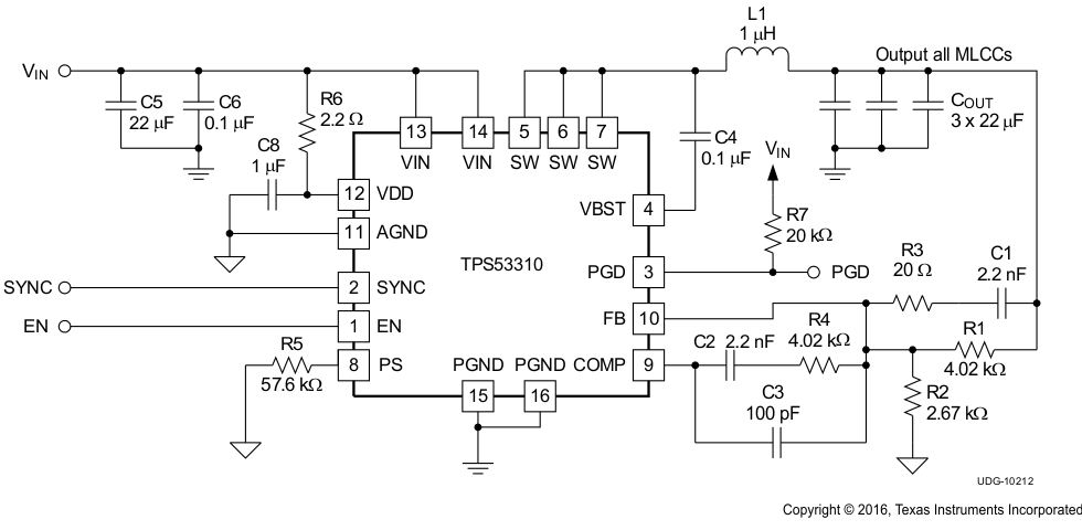
This design example describes a voltage-mode, 3-A synchronous buck converter with integrated MOSFETs. The device provides a fixed 1.5-V output at up to 3 A from a 3.3-V input bus.
8.2.1 Design Requirements
Table 2 lists the design specifications for the typical 3.3-V input example application.
Table 2. TPS53310 Design Example Specifications
| PARAMETER | CONDITIONS | MIN | TYP | MAX | UNIT |
|---|---|---|---|---|---|
| INPUT CHARACTERISTICS | |||||
| Input voltage, VIN | VIN | 2.9 | 3.3 | 6 | V |
| Input current | VIN = 3.3 V, 1.5 V/3 A | 2.82 | A | ||
| No load input current | VIN = 3.3 V, 1.5 V/0 A | 40 | mA | ||
| OUTPUT CHARACTERISTICS | |||||
| Output voltage, VO | 1.485 | 1.5 | 1.515 | V | |
| Output voltage regulation | Line regulation | 0.1% | |||
| Load regulation | 1% | ||||
| Output voltage ripple | VIN = 3.3 V, 1.5 V/0 A to 3 A | 20 | mVpp | ||
| Output load current | 0 | 3 | A | ||
| Output overcurrent | 4.5 | A | |||
| SYSTEMS CHARACTERISTICS | |||||
| Switching frequency | Fixed | 1.1 | MHz | ||
| 1.5-V full-load efficiency | VIN = 3.3 V, 1.5 V/3 A | 88.82% | |||
| VIN = 5 V, 1.5 V/3 A | 89.5% | ||||
| Operating temperature | 25 | °C | |||
8.2.2 Detailed Design Procedure
8.2.2.1 Determine the Value of R1 and R2
The output voltage is programmed by the voltage-divider resistor, R1 and R2 shown in Figure 13. R1 is connected between the FB pin and the output, and R2 is connected between the FB pin and GND. The recommended value for R1 is from 1 kΩ to 5 kΩ. Determine R2 using equation in Equation 1.

8.2.2.2 Choose the Inductor
The inductance value must be determined to give the ripple current of approximately 20% to 40% of maximum output current. The inductor ripple current is determined by Equation 2:

The inductor also requires low DCR to achieve good efficiency, as well as enough room above peak inductor current before saturation.
8.2.2.3 Choose the Output Capacitor(s)
The output capacitor selection is determined by output ripple and transient requirement. When operating in CCM, the output ripple has three components:


When ceramic output capacitors are used, the ESL component is usually negligible. In the case when multiple output capacitors are used, ESR and ESL must be the equivalent of ESR and ESL of all the output capacitor in parallel.
When operating in DCM, the output ripple is dominated by the component determined by capacitance. It also varies with load current and can be expressed as shown in Equation 7.

where
- α is the DCM on-time coefficient and can be expressed in Equation 8 (typical value 1.25)

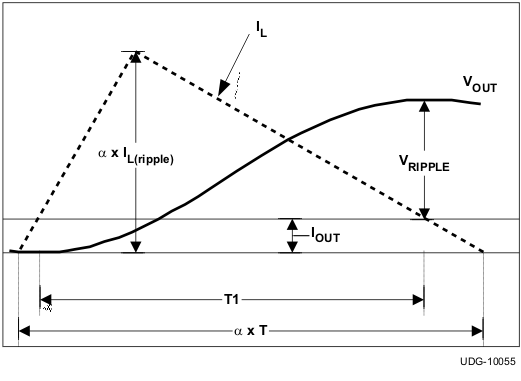 Figure 14. DCM VOUT Ripple Calculation
8.2.2.4 Choose the Input Capacitor
The selection of input capacitor must be determined by the ripple current requirement. The ripple current generated by the converter must be absorbed by the input capacitors as well as the input source. The RMS ripple current from the converter can be expressed in Equation 9.

To minimize the ripple current drawn from the input source, sufficient input decoupling capacitors must be placed close to the device. The ceramic capacitor is recommended because it provides low ESR and low ESL. The input voltage ripple can be calculated as shown in Equation 11 when the total input capacitance is determined.

8.2.2.5 Compensation Design
The TPS53310 uses voltage mode control. To effectively compensate the power stage and ensure fast transient response, Type III compensation is typically used.
The control to output transfer function can be described in Equation 12.

The output L-C filter introduces a double pole which can be calculated as shown in Equation 13.

The ESR zero can be calculated as shown in Equation 14.

Figure 15 and Figure 16 show the configuration of Type III compensation and typical pole and zero locations. Equation 16 through Equation 20 describe the compensator transfer function and poles and zeros of the Type III network.
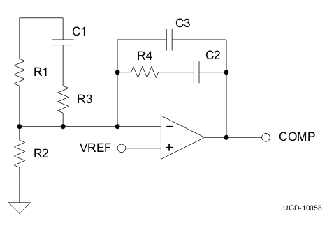 Figure 15. Type III Compensation Network
Configuration Schematic
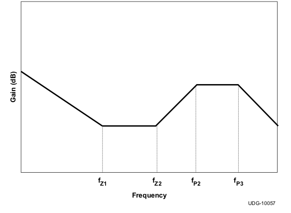 Figure 16. Type III Compensation Gain Plot
and Zero/Pole Placement


The two zeros can be placed near the double pole frequency to cancel the response from the double pole. One pole can be used to cancel ESR zero, and the other non-zero pole can be placed at half switching frequency to attenuate the high frequency noise and switching ripple. Suitable values can be selected to achieve a compromise between high phase margin and fast response. A phase margin higher than 45° is required for stable operation.
For DCM operation, a C3 between 56 pF and 150 pF is recommended for output capacitance between 20 µF to 200 µF.
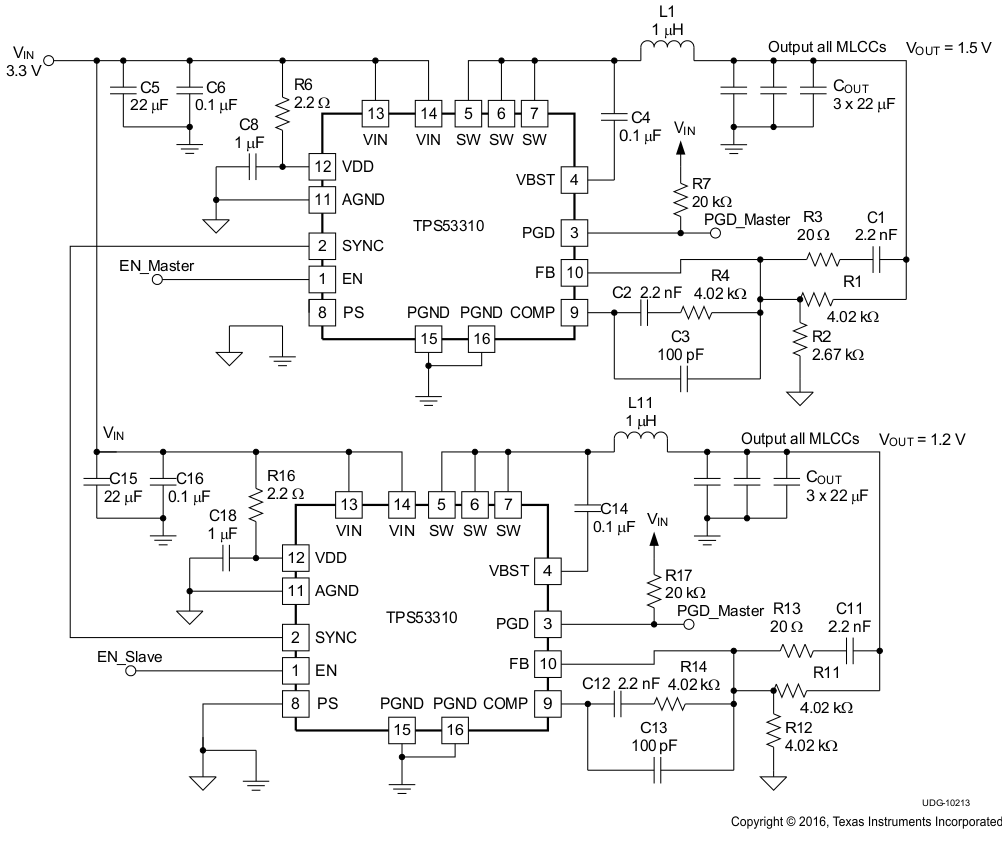
Figure 17 shows the master and slave configuration schematic for a design with a 3.3-V input.
8.2.3 Application Curves
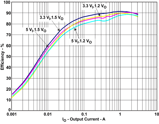
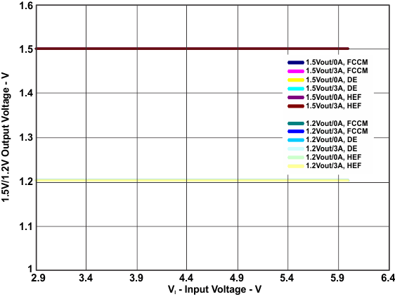 Figure 20. Line Regulation
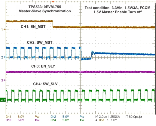 Figure 22. 1.5-V Master Turnoff During Master-Slave Synchronization (3.3 VIN, 1.5 V/3 A, 1.2 V/3 A
180° Synchronization, Then Turn Off Master)
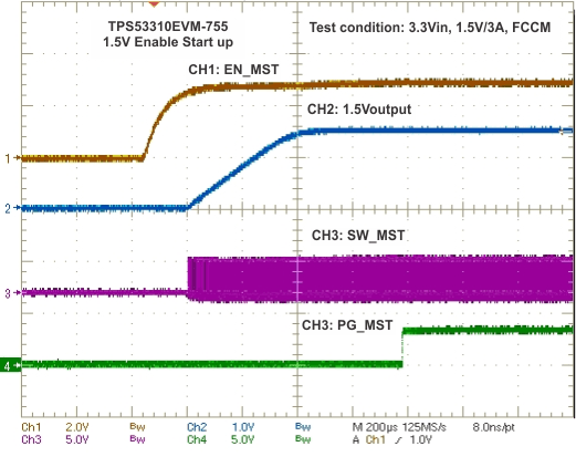 Figure 24. 1.5-V Turnon Waveform
(3.3 VIN, 1.5 V/3 A)
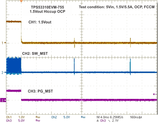 Figure 26. 1.5-V Hiccup OCP Waveform (5 VIN, 1.5 V/5.5 A OCP)
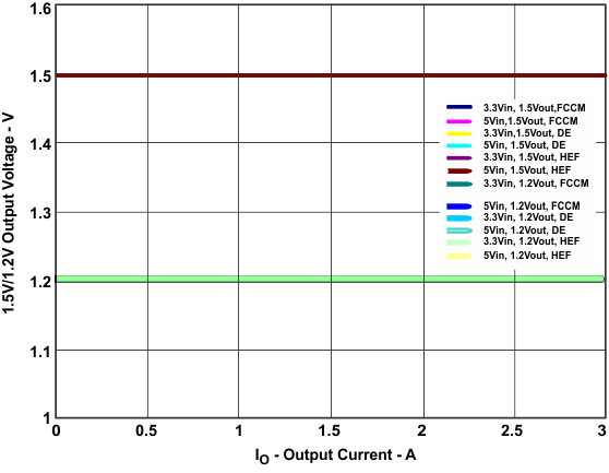
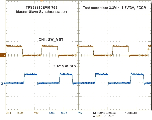 Figure 21. Master-Slave 180° Synchronization (3.3 VIN,
1.5 V/3 A, 1.2 V/3 A 180° Synchronization)
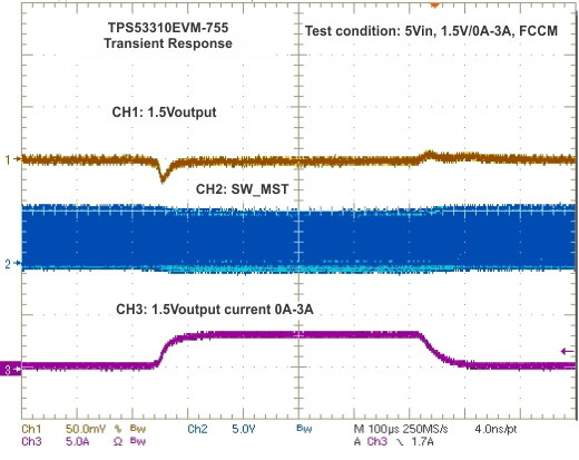 Figure 23. 1.5-V Turnon Waveform
(3.3 VIN, 1.5 V/3 A)
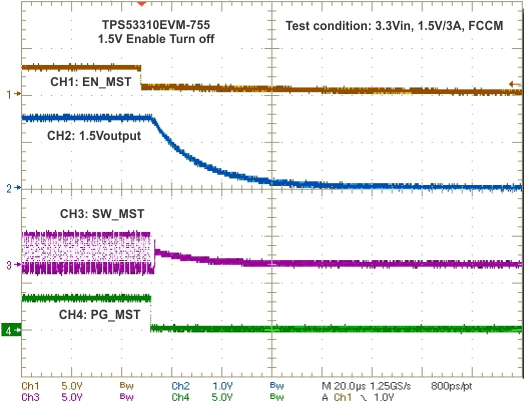 Figure 25. 1.5-V Turnoff Waveform
(3.3 VIN, 1.5 V/3 A)
