-
TPS54116-Q1 2.95-V to 6-V Input, 4-A Step-Down Converter and 1-A Source/Sink DDR Termination Regulator
- 1 Features
- 2 Applications
- 3 Description
- 4 Revision History
- 5 Pin Configuration and Functions
- 6 Specifications
-
7 Detailed Description
- 7.1 Overview
- 7.2 Functional Block Diagram
- 7.3
Feature Description
- 7.3.1 Fixed Frequency PWM Control
- 7.3.2 Bootstrap Voltage (BOOT) and Low Dropout Operation
- 7.3.3 Error Amplifier
- 7.3.4 Voltage Reference and Adjusting the Output Voltage
- 7.3.5 Enable and Adjusting Undervoltage Lockout
- 7.3.6 Soft Start and Tracking
- 7.3.7 Start-up into Pre-Biased Output
- 7.3.8 Power Good
- 7.3.9 Sequencing
- 7.3.10 Constant Switching Frequency and Timing Resistor (RT/SYNC)
- 7.3.11 Buck Overcurrent Protection
- 7.3.12 Overvoltage Transient Protection
- 7.3.13 VTT Sink and Source Regulator
- 7.3.14 VTTREF
- 7.3.15 Thermal Shutdown
- 7.4 Device Functional Modes
-
8 Application and Implementation
- 8.1 Application Information
- 8.2
Typical Application
- 8.2.1 Design Requirements
- 8.2.2
Detailed Design Procedure
- 8.2.2.1 Switching Frequency
- 8.2.2.2 Output Inductor Selection
- 8.2.2.3 Output Capacitor
- 8.2.2.4 Input Capacitor
- 8.2.2.5 Soft Start Capacitor
- 8.2.2.6 Undervoltage Lock Out Set Point
- 8.2.2.7 Bootstrap Capacitor
- 8.2.2.8 Power Good Pullup
- 8.2.2.9 ILIM Resistor
- 8.2.2.10 Output Voltage and Feedback Resistors Selection
- 8.2.2.11 Compensation
- 8.2.2.12 LDOIN Capacitor
- 8.2.2.13 VTTREF Capacitor
- 8.2.2.14 VTT Capacitor
- 8.2.3 Application Curves
- 9 Power Supply Recommendations
- 10Layout
- 11Device and Documentation Support
- 12Mechanical, Packaging, and Orderable Information
- IMPORTANT NOTICE
パッケージ・オプション
メカニカル・データ(パッケージ|ピン)
- RTW|24
サーマルパッド・メカニカル・データ
- RTW|24
発注情報
TPS54116-Q1 2.95-V to 6-V Input, 4-A Step-Down Converter and 1-A Source/Sink DDR Termination Regulator
1 Features
- AEC-Q100 Qualified With the Following Results:
- Device Temperature Grade 1: –40°C to +125°C Ambient Operating Temperature Range
- Device HBM ESD Classification Level 2
- Device CDM ESD Classification Level C6
- Single-chip DDR2, DDR3 and DDR3L Memory Power Solution
- 4-A Synchronous Buck Converter
- Integrated 33-mΩ High-side and 25-mΩ Low-side MOSFETs
- Fixed Frequency Current-mode Control
- Adjustable Frequency from 100 kHz to 2.5 MHz
- Synchronizable to an External Clock
- 0.6-V ±1% Voltage Reference Over Temperature
- Adjustable Cycle-by-Cycle Peak Current Limit
- Monotonic Start-up Into Pre-biased Outputs
- 1-A Source/Sink Termination LDO with ±20-mV DC Accuracy
- Stable with 2 × 10-µF MLCC Capacitor
- 10-mA Source/Sink Buffered Reference Output Regulated to Within 49% to 51% of VDDQ
- Independent Enable Pins with Adjustable UVLO and Hysteresis
- Thermal Shutdown
- -40°C to 150°C Operating TJ
- 24-pin, 4-mm x 4-mm WQFN Package
2 Applications
- DDR2, DDR3, DDR3L, and DDR4 Memory Power Supplies in Embedded Computing Systems
- SSTL_18, SSTL_15, SSTL_135, SSTL_12 and HSTL Termination
- Infotainment and Cluster
- Advanced Driver Assistance Systems (ADAS)
3 Description
The TPS54116-Q1 device is a full featured 6-V, 4-A, synchronous step down converter with two integrated MOSFETs and 1-A sink/source double data rate (DDR) VTT termination regulator with VTTREF buffered reference output.
The TPS54116-Q1 buck regulator minimizes solution size by integrating the MOSFETs and reducing inductor size with up to 2.5-MHz switching frequency. The switching frequency can be set above the medium wave radio band for noise sensitive applications and is synchronizable to an external clock. Synchronous rectification keeps the frequency fixed across the entire output load range. Efficiency is maximized through integrated 25-mΩ low-side and 33-mΩ high-side MOSFETs. Cycle-by-cycle peak current limit protects the device during an overcurrent condition and is adjustable with a resistor at the ILIM pin to optimize for smaller inductors.
The VTT termination regulator maintains fast transient response with only 2 × 10-µF ceramic output capacitance reducing external component count. The TPS54116-Q1 uses remote sensing of VTT for best regulation.
Using the enable pins to enter a shutdown mode reduces supply current to 1-µA. Under voltage lockout thresholds can be set with a resistor network on either enable pin. The VTT and VTTREF outputs are discharged when disabled with ENLDO.
Full integration minimizes the IC footprint with a small 4 mm × 4 mm thermally enhanced WQFN package.
Device Information(1)
| PART NUMBER | PACKAGE | BODY SIZE (NOM) |
|---|---|---|
| TPS54116-Q1 | WQFN (24) | 4.00 mm × 4.00 mm |
- For all available packages, see the orderable addendum at the end of the datasheet.
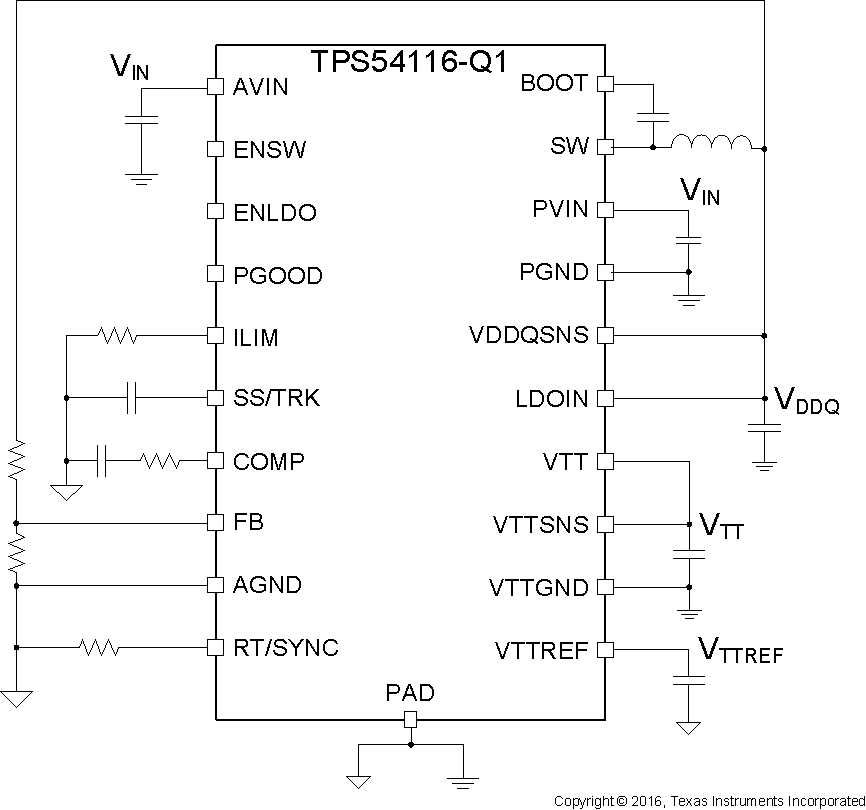
Simplified Schematic

4 Revision History
Changes from A Revision (August 2016) to B Revision
- Changed text From: "double date rate (DDR)" To: "double data rate (DDR)" in the DescriptionGo
Changes from * Revision (August 2016) to A Revision
5 Pin Configuration and Functions
