SLVS996D September 2009 – September 2015 TPS54262-Q1
PRODUCTION DATA.
- 1 Features
- 2 Applications
- 3 Description
- 4 Revision History
- 5 Pin Configuration and Functions
- 6 Specifications
-
7 Detailed Description
- 7.1 Overview
- 7.2 Functional Block Diagram
- 7.3
Feature Description
- 7.3.1 Unregulated Input Voltage
- 7.3.2 Regulated Output Voltage
- 7.3.3 Regulation and Feedback Voltage
- 7.3.4 Enable and Shutdown
- 7.3.5 Soft Start
- 7.3.6 Oscillator Frequency
- 7.3.7 Slew Rate Control
- 7.3.8 Reset
- 7.3.9 Reset Delay
- 7.3.10 Reset Threshold and Undervoltage Threshold
- 7.3.11 Overvoltage Supervisor
- 7.3.12 Noise Filter on RST_TH and OV_TH Terminals
- 7.3.13 Boot Capacitor
- 7.3.14 Short Circuit Protection
- 7.3.15 Overcurrent Protection
- 7.3.16 Internal Undervoltage Lockout (UVLO)
- 7.3.17 Thermal Shutdown (TSD)
- 7.3.18 Loop Control Frequency Compensation - Type 3
- 7.4 Device Functional Modes
-
8 Application and Implementation
- 8.1 Application Information
- 8.2
Typical Application
- 8.2.1 Design Requirements
- 8.2.2
Detailed Design Procedure
- 8.2.2.1
Component Selection
- 8.2.2.1.1 Input Capacitors (C1, C11)
- 8.2.2.1.2 Output Capacitor (C4, C12)
- 8.2.2.1.3 Soft-Start Capacitor (C6)
- 8.2.2.1.4 Bootstrap Capacitor (C3)
- 8.2.2.1.5 Power-On Reset Delay (PORdly) Capacitor (C2)
- 8.2.2.1.6 Output Inductor (L1)
- 8.2.2.1.7 Flyback Schottky Diode (D2)
- 8.2.2.1.8 Resistor to Set Slew Rate (R7)
- 8.2.2.1.9 Resistor to Select Switching Frequency (R8)
- 8.2.2.1.10 Resistors to Select Output Voltage (R4, R5)
- 8.2.2.1.11 Resistors to Set Undervoltage, Overvoltage, and Reset Thresholds (R1, R2, R3)
- 8.2.2.1.12 Low-Power Mode (LPM) Threshold
- 8.2.2.1.13 Enable Pin Pull-Up Resistor (R11) and Voltage Divider Resistor (R10)
- 8.2.2.1.14 Pull-Up Resistor (R12) at RST Pin
- 8.2.2.1.15 Type 3 Compensation Components (R5, R6, R9, C5, C7, C8)
- 8.2.2.1.16 Noise Filter on RST_TH and OV_TH Terminals (C9, C10)
- 8.2.2.2
Design Example 1
- 8.2.2.2.1 Calculate the Switching Frequency (fsw)
- 8.2.2.2.2 Calculate the Ripple Current (IRipple)
- 8.2.2.2.3 Calculate the Inductor Value (L1)
- 8.2.2.2.4 Calculate the Output Capacitor and ESR (C4)
- 8.2.2.2.5 Calculate the Feedback Resistors (R4, R5)
- 8.2.2.2.6 Calculate Type 3 Compensation Components
- 8.2.2.2.7 Calculate Soft-Start Capacitor (C6)
- 8.2.2.2.8 Calculate Bootstrap Capacitor (C3)
- 8.2.2.2.9 Calculate Power-On Reset Delay Capacitor (C2)
- 8.2.2.2.10 Calculate Input Capacitor (C1, C11)
- 8.2.2.2.11 Calculate Resistors to Control Slew Rate (R7)
- 8.2.2.2.12 Resistors to Select Undervoltage, Overvoltage and Reset Threshold Values (R1, R2, R3)
- 8.2.2.2.13 Diode D1 and D2 Selection
- 8.2.2.2.14 Noise Filter on RST_TH and OV_TH Terminals (C9 and C10)
- 8.2.2.2.15 Power Budget and Temperature Estimation
- 8.2.2.3
Design Example 2
- 8.2.2.3.1 Calculate the Switching Frequency (fsw)
- 8.2.2.3.2 Calculate the Ripple Current (IRipple)
- 8.2.2.3.3 Calculate the Inductor Value (L1)
- 8.2.2.3.4 Calculate the Output Capacitor and ESR (C4, C12)
- 8.2.2.3.5 Calculate the Feedback Resistors (R4, R5)
- 8.2.2.3.6 Calculate Type 3 Compensation Components
- 8.2.2.3.7 Calculate Soft-Start Capacitor (C6)
- 8.2.2.3.8 Calculate Bootstrap Capacitor (C3)
- 8.2.2.3.9 Calculate Power-On Reset Delay Capacitor (C2)
- 8.2.2.3.10 Calculate Input Capacitor (C1, C11)
- 8.2.2.3.11 Calculate Resistors to Control Slew Rate (R7)
- 8.2.2.3.12 Resistors to Select Undervoltage, Overvoltage and Reset Threshold Values (R1, R2, R3)
- 8.2.2.3.13 Diode D1 and D2 Selection
- 8.2.2.3.14 Noise Filter on RST_TH and OV_TH Terminals (C9 and C10)
- 8.2.2.3.15 Power Budget and Temperature Estimation
- 8.2.2.1
Component Selection
- 8.2.3 Application Curves
- 9 Power Supply Recommendations
- 10Layout
- 11Device and Documentation Support
- 12Mechanical, Packaging, and Orderable Information
パッケージ・オプション
メカニカル・データ(パッケージ|ピン)
- PWP|20
サーマルパッド・メカニカル・データ
- PWP|20
発注情報
1 Features
- Asynchronous Switch Mode Regulator
- Qualified for Automotive Applications
- 3.6-V to 48-V Operating Range, Withstands Transients up to 60 V
- 2-A Maximum Load Current
- 50-µA Typical Quiescent Current
- 200-kHz to 2.2-MHz Switching Frequency
- 0.8 V ± 1.5% Voltage Reference
- High-Voltage Tolerant Enable Input
- Soft Start on Enable Cycle
- Slew Rate Control on Internal Power Switch
- Low-Power Mode for Light-Load Conditions
- Programmable Delay for Power-On Reset
- External Compensation for Error Amplifier
- Reset Function Filter Time for Fast Negative Transients
- Programmable Overvoltage, Undervoltage Output Monitor
- Thermal Sensing and Shutdown
- Switch Current Limit Protection
- Short Circuit and Overcurrent Protection of FET
- Junction Temperature Range: –40°C to 150°C
- 20-Pin HTSSOP PowerPAD™ Package
2 Applications
3 Description
The TPS54262-Q1 device is a 60-V, 2-A step-down switch-mode power supply with a low-power mode and a programmable voltage supervisor with an integrated NMOS switching FET. Integrated input voltage line feed forward topology improves line transient regulation of the voltage mode buck regulator. The regulator has a cycle-by-cycle current limit. The device also features low-power mode operation under light-load conditions which reduces the supply current to 50 µA (typical). By pulling the EN pin low, the supply shutdown current is reduced to 1 µA (typical).
An open-drain reset signal indicates when the nominal output drops below the reset threshold set by an external resistor divider network. The output voltage start-up ramp is controlled by a soft-start capacitor. There is an internal undervoltage shut down which is activated when the input supply ramps down to 2.6 V. The device features a short circuit protection circuit which protects the device during overload condition, and also has a thermal shutdown protection.
Device Information(1)
| PART NUMBER | PACKAGE | BODY SIZE (NOM) |
|---|---|---|
| TPS54262-Q1 | HTSSOP (20) | 6.50 mm × 4.40 mm |
- For all available packages, see the orderable addendum at the end of the data sheet.
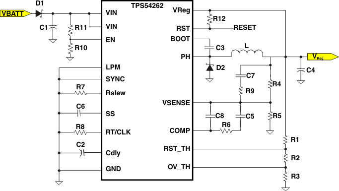
Typical Application Schematic

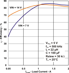
Typical Converter Efficiency
