SLUSC26A May 2015 – February 2016 TPS54334
PRODUCTION DATA.
- 1 Features
- 2 Applications
- 3 Description
- 4 Revision History
- 5 Pin Configuration and Functions
- 6 Specifications
-
7 Detailed Description
- 7.1 Overview
- 7.2 Functional Block Diagram
- 7.3
Feature Description
- 7.3.1 Fixed Frequency PWM Control
- 7.3.2 Light Load Operation
- 7.3.3 Slope Compensation and Output Current
- 7.3.4 Bootstrap Voltage (BOOT) and Low Dropout Operation
- 7.3.5 Error Amplifier
- 7.3.6 Voltage Reference
- 7.3.7 Adjusting the Output Voltage
- 7.3.8 Enable and Undervoltage Lockout
- 7.3.9 Slow Start
- 7.3.10 Safe Start-up into Pre-Biased Outputs
- 7.3.11 Power Good (PGOOD)
- 7.4 Device Functional Modes
-
8 Application and Implementation
- 8.1 Application Information
- 8.2
Typical Applications
- 8.2.1
TPS54334 Application
- 8.2.1.1 Design Requirements
- 8.2.1.2 Detailed Design Procedure
- 8.2.1.3 Application Curves
- 8.2.1
TPS54334 Application
- 9 Power Supply Recommendations
- 10Layout
- 11Device and Documentation Support
- 12Mechanical, Packaging, and Orderable Information
パッケージ・オプション
メカニカル・データ(パッケージ|ピン)
サーマルパッド・メカニカル・データ
- DDA|8
発注情報
10 Layout
10.1 Layout Guidelines
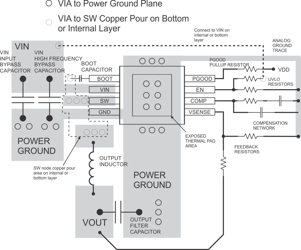
The VIN pin should be bypassed to ground with a low ESR ceramic bypass capacitor. Care should be taken to minimize the loop area formed by the bypass capacitor connection. the VIN pin, and the GND pin of the IC. The typical recommended bypass capacitance is 10-μF ceramic with a X5R or X7R dielectric and the optimum placement is closest to the VIN and GND pins of the device. See Figure 34 for a PCB layout example. The GND pin should be tied to the PCB ground plane at the pin of the IC. To facilitate close placement of the input bypass capacitors, The SW pin should be routed to a small copper area directly adjacent to the pin. Use vias to rout the SW signal to the bottom side or an inner layer. If necessary you can allow the top side copper area to extend slightly under the body of the closest input bypass capacitor. Make the copper trace on the bottom or internal layer short and wide as practical to reduce EMI issues. Connect the trace with vias back to the top side to connect with the output inductor as shown after the GND pin. In the same way use a bottom or internal layer trace to rout the SW signal across the VIN pin to connect to the BOOT capacitor as shown. Make the circulating loop from SW to the output inductor, output capacitors and back to GND as tight as possible while preserving adequate etch width to reduce conduction losses in the copper.
For operation at full rated load, the ground area near the IC must provide adequate heat dissipating area. Connect the exposed thermal pad to bottom or internal layer ground plane using vias as shown. Additional vias may be used adjacent to the IC to tie top side copper to the internal or bottom layer copper. The additional external components can be placed approximately as shown. Use a separate ground trace to connect the feedback, compensation, UVLO and RT returns. Connect this ground trace to the main power ground at a single point to minimize circulating currents. It may be possible to obtain acceptable performance with alternate layout schemes, however this layout has been shown to produce good results and is intended as a guideline.
10.2 Layout Example
 Figure 34. TPS54334DDA Board Layout