SLUSC26A May 2015 – February 2016 TPS54334
PRODUCTION DATA.
- 1 Features
- 2 Applications
- 3 Description
- 4 Revision History
- 5 Pin Configuration and Functions
- 6 Specifications
-
7 Detailed Description
- 7.1 Overview
- 7.2 Functional Block Diagram
- 7.3
Feature Description
- 7.3.1 Fixed Frequency PWM Control
- 7.3.2 Light Load Operation
- 7.3.3 Slope Compensation and Output Current
- 7.3.4 Bootstrap Voltage (BOOT) and Low Dropout Operation
- 7.3.5 Error Amplifier
- 7.3.6 Voltage Reference
- 7.3.7 Adjusting the Output Voltage
- 7.3.8 Enable and Undervoltage Lockout
- 7.3.9 Slow Start
- 7.3.10 Safe Start-up into Pre-Biased Outputs
- 7.3.11 Power Good (PGOOD)
- 7.4 Device Functional Modes
-
8 Application and Implementation
- 8.1 Application Information
- 8.2
Typical Applications
- 8.2.1
TPS54334 Application
- 8.2.1.1 Design Requirements
- 8.2.1.2 Detailed Design Procedure
- 8.2.1.3 Application Curves
- 8.2.1
TPS54334 Application
- 9 Power Supply Recommendations
- 10Layout
- 11Device and Documentation Support
- 12Mechanical, Packaging, and Orderable Information
パッケージ・オプション
メカニカル・データ(パッケージ|ピン)
サーマルパッド・メカニカル・データ
- DDA|8
発注情報
5 Pin Configuration and Functions
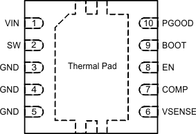
DRC Package
10 Pin VSON
Top View

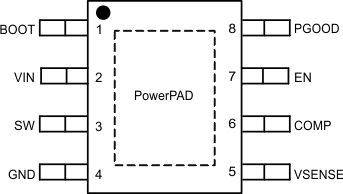
DDA Package
8 Pin SO
Top View

Pin Functions
| PIN NAME | NUMBER | I/O | DESCRIPTION | |
|---|---|---|---|---|
| DDA | DRC | |||
| BOOT | 1 | 9 | O | A bootstrap capacitor is required between BOOT and SW. If the voltage on this capacitor is below the minimum required by the output device, the output is forced to switch off until the capacitor is refreshed. |
| COMP | 6 | 7 | O | Error amplifier output, and input to the output switch current comparator. Connect frequency compensation components to this pin. |
| EN | 7 | 8 | I | Enable pin. Float to enable. |
| GND | 4 | 3, 4, 5 | – | Ground. |
| PGOOD | 8 | 10 | O | PGOOD open drain output. Connect a pull-up resistor with a value of 100kΩ to this pin. |
| SW | 3 | 2 | O | The source of the internal high side power MOSFET. |
| Vin | 2 | 1 | – | Input supply voltage, 4.2 V to 28 V. |
| VSENSE | 5 | 6 | I | Inverting node of the gm error amplifier. |
| PowerPad (SO only) | – | GND pin should be connected to the exposed thermal pad for proper operation. This thermal pad should be connected to any internal PCB ground plane using multiple vias for good thermal performance. | ||
| Thermal pad (VSON only) | ||||