JAJSCB1 July 2016 TPS54335-2A
PRODUCTION DATA.
- 1 特長
- 2 アプリケーション
- 3 概要
- 4 改訂履歴
- 5 Pin Configuration and Functions
- 6 Specifications
-
7 Detailed Description
- 7.1 Overview
- 7.2 Functional Block Diagram
- 7.3
Feature Description
- 7.3.1 Fixed-Frequency PWM Control
- 7.3.2 Light-Load Operation
- 7.3.3 Voltage Reference
- 7.3.4 Adjusting the Output Voltage
- 7.3.5 Enabling and Adjusting Undervoltage Lockout
- 7.3.6 Error Amplifier
- 7.3.7 Slope Compensation and Output Current
- 7.3.8 Safe Startup into Pre-Biased Outputs
- 7.3.9 Bootstrap Voltage (BOOT)
- 7.3.10 Output Overvoltage Protection (OVP)
- 7.3.11 Overcurrent Protection
- 7.3.12 Thermal Shutdown
- 7.3.13 Small-Signal Model for Loop Response
- 7.3.14 Simple Small-Signal Model for Peak Current-Mode Control
- 7.3.15 Small-Signal Model for Frequency Compensation
- 7.4 Device Functional Modes
-
8 Application and Implementation
- 8.1 Application Information
- 8.2
Typical Applications
- 8.2.1 Design Requirements
- 8.2.2 Detailed Design Procedure
- 8.2.3 Application Curves
- 9 Power Supply Recommendations
- 10Layout
- 11デバイスおよびドキュメントのサポート
- 12メカニカル、パッケージ、および注文情報
5 Pin Configuration and Functions
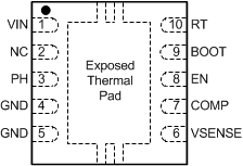
DRC Package
10-Pin VSON With Exposed Thermal Pad
Top View

Pin Functions
| PIN | I/O | DESCRIPTION | |
|---|---|---|---|
| NAME | VSON | ||
| BOOT | 9 | O | A bootstrap capacitor is required between the BOOT and PH pins. If the voltage on this capacitor is below the minimum required by the output device, the output is forced to switch off until the capacitor is refreshed. |
| COMP | 7 | O | This pin is the error-amplifier output and the input to the output switch-current comparator. Connect frequency compensation components to this pin. |
| EN | 8 | I | This pin is the enable pin. Float the EN pin to enable. |
| NC | 2 | — | No Connect |
| GND | 4 | — | Ground |
| GND | 5 | — | Ground |
| PH | 3 | O | The PH pin is the source of the internal high-side power MOSFET. |
| RT | 10 | O | Connect the RT pin to an external timing resistor to adjust the switching frequency of the device. |
| VIN | 1 | — | This pin is the 4.5-V to 28-V input supply voltage. |
| VSENSE | 6 | I | This pin is the inverting node of the transconductance (gm) error amplifier. |
| Thermal pad | — | For proper operation, connect the GND pin to the exposed thermal pad. This thermal pad should be connected to any internal PCB ground plane using multiple vias for good thermal performance. | |