JAJSCB1 July 2016 TPS54335-2A
PRODUCTION DATA.
- 1 特長
- 2 アプリケーション
- 3 概要
- 4 改訂履歴
- 5 Pin Configuration and Functions
- 6 Specifications
-
7 Detailed Description
- 7.1 Overview
- 7.2 Functional Block Diagram
- 7.3
Feature Description
- 7.3.1 Fixed-Frequency PWM Control
- 7.3.2 Light-Load Operation
- 7.3.3 Voltage Reference
- 7.3.4 Adjusting the Output Voltage
- 7.3.5 Enabling and Adjusting Undervoltage Lockout
- 7.3.6 Error Amplifier
- 7.3.7 Slope Compensation and Output Current
- 7.3.8 Safe Startup into Pre-Biased Outputs
- 7.3.9 Bootstrap Voltage (BOOT)
- 7.3.10 Output Overvoltage Protection (OVP)
- 7.3.11 Overcurrent Protection
- 7.3.12 Thermal Shutdown
- 7.3.13 Small-Signal Model for Loop Response
- 7.3.14 Simple Small-Signal Model for Peak Current-Mode Control
- 7.3.15 Small-Signal Model for Frequency Compensation
- 7.4 Device Functional Modes
-
8 Application and Implementation
- 8.1 Application Information
- 8.2
Typical Applications
- 8.2.1 Design Requirements
- 8.2.2 Detailed Design Procedure
- 8.2.3 Application Curves
- 9 Power Supply Recommendations
- 10Layout
- 11デバイスおよびドキュメントのサポート
- 12メカニカル、パッケージ、および注文情報
6 Specifications
6.1 Absolute Maximum Ratings(1)
| MIN | MAX | UNIT | ||
|---|---|---|---|---|
| Input voltage | VIN | –0.3 | 30 | V |
| EN | –0.3 | 6 | V | |
| BOOT | –0.3 | (VPH + 7.5) | V | |
| VSENSE | –0.3 | 3 | V | |
| COMP | –0.3 | 3 | V | |
| RT | –0.3 | 3 | V | |
| Output voltage | BOOT-PH | 0 | 7.5 | V |
| PH | –1 | 30 | V | |
| PH, 10-ns transient | –3.5 | 30 | V | |
| VDIFF (GND to exposed thermal pad) | –0.2 | 0.2 | V | |
| Source current | EN | 100 | 100 | µA |
| RT | 100 | 100 | µA | |
| PH | Current-limit | A | ||
| Sink current | PH | Current-limit | A | |
| COMP | 200 | 200 | µA | |
| Operating junction temperature | –40 | 150 | °C | |
| Storage temperature, Tstg | –65 | 150 | °C | |
(1) Stresses beyond those listed under the absolute maximum ratings may cause permanent damage to the device. These are stress ratings only, and functional operation of the device at these or any other conditions beyond those indicated under the recommended operating conditions is not implied. Exposure to absolute-maximum-rated conditions for extended periods may affect device reliability.
6.2 ESD Ratings
| VALUE | UNIT | |||
|---|---|---|---|---|
| V(ESD) | Electrostatic discharge | Human body model (HBM), per ANSI/ESDA/JEDEC JS–001, all pins(1) | 2000 | V |
| Charged device model (CDM), per JEDEC specification JESD22-C101, all pins(2) | 500 | |||
(1) JEDEC document JEP155 states that 500-V HBM allows safe manufacturing with a standard ESD control process.
(2) JEDEC document JEP157 states that 250-V CDM allows safe manufacturing with a standard ESD control process.
6.3 Recommended Operating Conditions
over operating free-air temperature range (unless otherwise noted)| MIN | MAX | UNIT | |||
|---|---|---|---|---|---|
| VSS | Supply input voltage | 4.5 | 28 | V | |
| VOUT | Output voltage | 0.8 | 24 | V | |
| IOUT | Output current | 0 | 3 | A | |
| TJ | Operating junction temperature(1) | –40 | 150 | °C | |
(1) The device must operate within 150°C to ensure continuous function and operation of the device.
6.4 Thermal Information
over operating free-air temperature range (unless otherwise noted)| THERMAL METRIC | TPS54335-2A | UNIT | |
|---|---|---|---|
| DRC (VSON) | |||
| 10 PINS | |||
| RθJA | Junction-to-ambient thermal resistance | 43.9 | °C/W |
| RθJC(top) | Junction-to-case (top) thermal resistance | 55.4 | °C/W |
| RθJB | Junction-to-board thermal resistance | 18.9 | °C/W |
| ψJT | Junction-to-top characterization parameter | 0.7 | °C/W |
| ψJB | Junction-to-board characterization parameter | 19.1 | °C/W |
| RθJC(bot) | Junction-to-case (bottom) thermal resistance | 5.3 | °C/W |
6.5 Electrical Characteristics
The electrical ratings specified in this section apply to all specifications in this document unless otherwise noted. These specifications are interpreted as conditions that will not degrade the parametric or functional specifications of the device for the life of the product containing it. TJ = –40°C to 150°C, V = 4.5 to 28 V, (unless otherwise noted)| PARAMETER | TEST CONDITIONS | MIN | TYP | MAX | UNIT | |
|---|---|---|---|---|---|---|
| SUPPLY VOLTAGE AND UVLO (VIN PIN) | ||||||
| Operating input voltage | 4.5 | 28 | V | |||
| Input UVLO threshold | Rising V | 4 | 4.5 | V | ||
| Input UVLO hysteresis | 180 | 400 | mV | |||
| VIN-shutdown supply current | = 0 V | 2 | 10 | µA | ||
| VIN-operating non-switching supply current | = 810 mV | 310 | 800 | µA | ||
| ENABLE (EN PIN) | ||||||
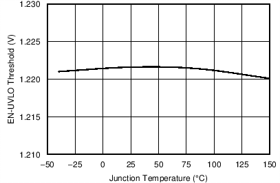
| Enable threshold | Rising | 1.21 | 1.28 | V | ||
| Enable threshold | Falling | 1.1 | 1.17 | V | ||
| Input current | = 1.1 V | 1.15 | µA | |||
| Hysteresis current | = 1.3 V | 3.3 | µA | |||
| VOLTAGE REFERENCE | ||||||
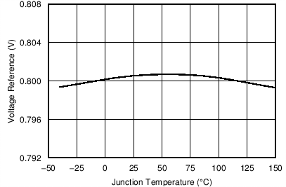
| Reference | TJ =25°C | 0.7936 | 0.8 | 0.8064 | V | |
| 0.788 | 0.8 | 0.812 | ||||
| MOSFET | ||||||
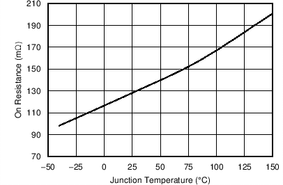
| High-side switch resistance(1) | = 3 V | 160 | 280 | mΩ | ||
| = 6 V | 128 | 230 | mΩ | |||
| Low-side switch resistance(1) | V = 12 V | 84 | 170 | mΩ | ||
| ERROR AMPLIFIER | ||||||
| Error-amplifier transconductance (gm) | –2 µA < ICOMP < 2 µA, VCOMP = 1 V | 1300 | µmhos | |||
| Error-amplifier source and sink | VCOMP = 1 V, 100-mV overdrive | 100 | µA | |||
| Start switching peak current threshold(2) | 0.5 | A | ||||
| COMP to ISWITCH gm | 8 | A/V | ||||
| CURRENT-LIMIT | ||||||
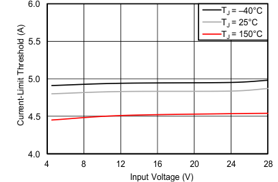
| High-side switch current-limit threshold | 4 | 4.9 | 6.5 | A | ||
| Low-side switch sourcing current-limit | 3.5 | 4.7 | 6.1 | A | ||
| Low-side switch sinking current-limit | 0 | A | ||||
| THERMAL SHUTDOWN | ||||||
| Thermal shutdown(2) | 160 | 175 | °C | |||
| Thermal shutdown hysteresis(2) | 10 | °C | ||||
| BOOT PIN | ||||||
| BOOT-PH UVLO | 2.1 | 3 | V | |||
(1) Measured at pins
(2) Not production tested.
6.6 Timing Requirements
| MIN | TYP | MAX | UNIT | |||
|---|---|---|---|---|---|---|
| CURRENT-LIMIT | ||||||
| Hiccup wait time | 512 | Cycles | ||||
| Hiccup time before restart | 16384 | Cycles | ||||
| THERMAL SHUTDOWN | ||||||
| Thermal shutdown hiccup time | 32768 | Cycles | ||||
| SOFT START | ||||||
| Internal soft-start time, TPS54335-2A | 2 | ms | ||||
6.7 Switching Characteristics
over operating free-air temperature range (unless otherwise noted)| PARAMETER | TEST CONDITIONS | MIN | TYP | MAX | UNIT | |
|---|---|---|---|---|---|---|
| PH PIN | ||||||
| Minimum on time | Measured at 90% to 90% of VIN, IPH = 2 A | 94 | 145 | ns | ||
| Minimum off time | ≥ 3 V | 0% | ||||
| SWITCHING FREQUENCY | ||||||
| Switching frequency range, TPS54335-2A | 50 | 1500 | kHz | |||
| R = 100 kΩ | 384 | 480 | 576 | kHz | ||
| R = 1000 kΩ, –40°C to 105°C | 40 | 50 | 60 | kHz | ||
| R = 30 kΩ | 1200 | 1500 | 1800 | kHz | ||
6.8 Typical Characteristics
| VIN = 12 V | ||
| VIN = 12 V | ||
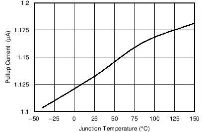
| VIN = 12 V | ||
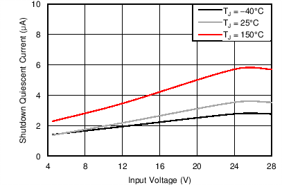
| VEN = 0 V | ||
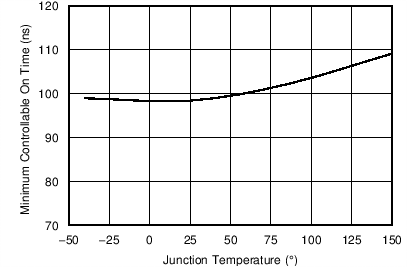
| VIN = 12 V | ||
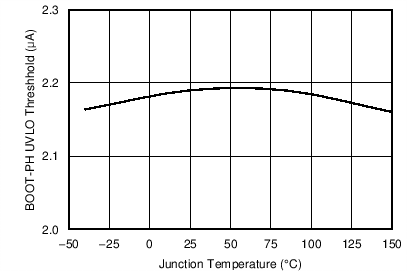
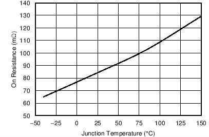
| VIN = 12 V | ||
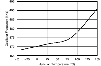

| VIN = 12 V | ||
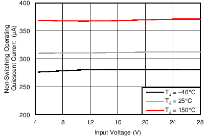

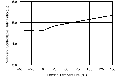
| VIN = 12 V | ||
