JAJSGM6 December 2018 TPS54360B
PRODUCTION DATA.
- 1 特長
- 2 アプリケーション
- 3 概要
- 4 改訂履歴
- 5 概要(続き)
- 6 Pin Configuration and Functions
- 7 Specifications
-
8 Detailed Description
- 8.1 Overview
- 8.2 Functional Block Diagram
- 8.3
Feature Description
- 8.3.1 Fixed Frequency PWM Control
- 8.3.2 Slope Compensation Output Current
- 8.3.3 Pulse Skip Eco-mode
- 8.3.4 Low Dropout Operation and Bootstrap Voltage (BOOT)
- 8.3.5 Error Amplifier
- 8.3.6 Adjusting the Output Voltage
- 8.3.7 Enable and Adjusting Undervoltage Lockout
- 8.3.8 Internal Soft Start
- 8.3.9 Constant Switching Frequency and Timing Resistor (RT/CLK) pin)
- 8.3.10 Accurate Current Limit Operation and Maximum Switching Frequency
- 8.3.11 Synchronization to RT/CLK pin
- 8.3.12 Overvoltage Protection
- 8.3.13 Thermal Shutdown
- 8.3.14 Small Signal Model for Loop Response
- 8.3.15 Simple Small Signal Model for Peak-Current-Mode Control
- 8.3.16 Small Signal Model for Frequency Compensation
- 8.4 Device Functional Modes
-
9 Application and Implementation
- 9.1 Application Information
- 9.2
Typical Application
- 9.2.1 Design Requirements
- 9.2.2
Detailed Design Procedure
- 9.2.2.1 Custom Design with WEBENCH® Tools
- 9.2.2.2 Selecting the Switching Frequency
- 9.2.2.3 Output Inductor Selection (LO)
- 9.2.2.4 Output Capacitor
- 9.2.2.5 Catch Diode
- 9.2.2.6 Input Capacitor
- 9.2.2.7 Bootstrap Capacitor Selection
- 9.2.2.8 Undervoltage Lockout Set Point
- 9.2.2.9 Output Voltage and Feedback Resistors Selection
- 9.2.2.10 Minimum VIN
- 9.2.2.11 Compensation
- 9.2.2.12 Discontinuous Conduction Mode and Eco-mode Boundary
- 9.2.2.13 Power Dissipation Estimate
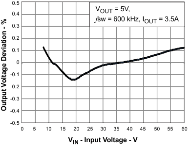
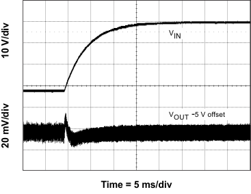
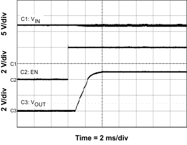
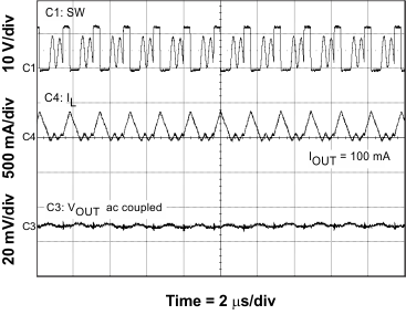
- 9.2.3 Application Curves
- 9.3 Other Applications
- 10Power Supply Recommendations
- 11Layout
- 12デバイスおよびドキュメントのサポート
- 13メカニカル、パッケージ、および注文情報
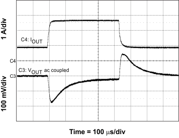
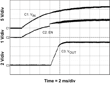
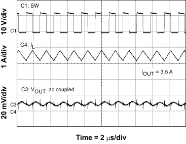
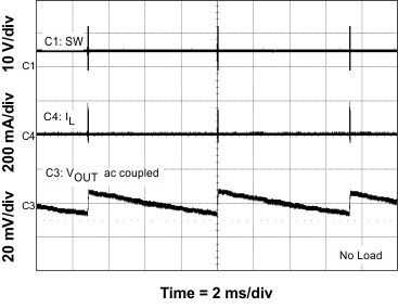
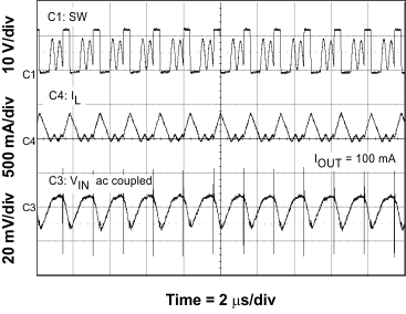
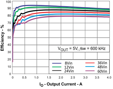
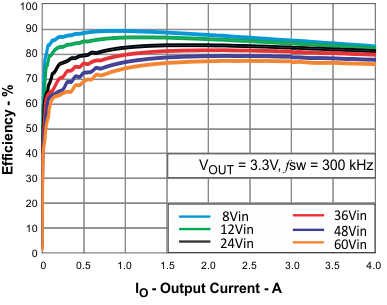
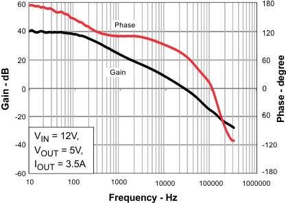
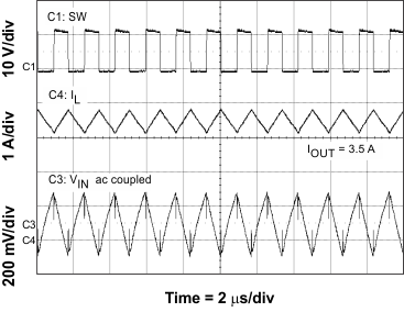
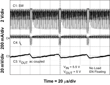
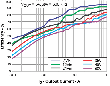
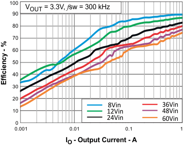
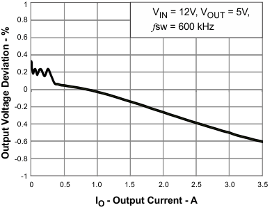
9.2.3 Application Curves
