SLVSCC4B April 2014 – January 2017 TPS54361-Q1
PRODUCTION DATA.
- 1 Features
- 2 Applications
- 3 Description
- 4 Revision History
- 5 Pin Configuration and Functions
- 6 Specifications
-
7 Detailed Description
- 7.1 Overview
- 7.2 Functional Block Diagram
- 7.3
Feature Description
- 7.3.1 Fixed-Frequency PWM Control
- 7.3.2 Slope Compensation Output Current
- 7.3.3 Pulse-Skip Eco-mode
- 7.3.4 Low Dropout Operation and Bootstrap Voltage (BOOT)
- 7.3.5 Error Amplifier
- 7.3.6 Adjusting the Output Voltage
- 7.3.7 Enable and Adjust Undervoltage Lockout
- 7.3.8 Soft-Start/Tracking Pin (SS/TR)
- 7.3.9 Sequencing
- 7.3.10 Constant Switching Frequency and Timing Resistor (RT/CLK) Pin)
- 7.3.11 Accurate Current-Limit Operation and Maximum Switching Frequency
- 7.3.12 Synchronization to RT/CLK Pin
- 7.3.13 Power Good (PWRGD Pin)
- 7.3.14 Overvoltage Protection
- 7.3.15 Thermal Shutdown
- 7.3.16 Small Signal Model for Loop Response
- 7.3.17 Simple Small Signal Model for Peak Current Mode Control
- 7.3.18 Small Signal Model for Frequency Compensation
- 7.4 Device Functional Modes
-
8 Application and Implementation
- 8.1 Application Information
- 8.2
Typical Application
- 8.2.1 Design Requirements
- 8.2.2
Detailed Design Procedure
- 8.2.2.1 Custom Design with WEBENCH® Tools
- 8.2.2.2 Selecting the Switching Frequency
- 8.2.2.3 Output Inductor Selection (LO)
- 8.2.2.4 Output Capacitor
- 8.2.2.5 Catch Diode
- 8.2.2.6 Input Capacitor
- 8.2.2.7 Slow-Start Capacitor
- 8.2.2.8 Bootstrap Capacitor Selection
- 8.2.2.9 Undervoltage Lockout Set Point
- 8.2.2.10 Output Voltage and Feedback Resistors Selection
- 8.2.2.11 Compensation
- 8.2.2.12 Discontinuous Conduction Mode and Eco-mode Boundary
- 8.2.3 Application Curves
- 9 Power Supply Recommendations
- 10Layout
- 11Device and Documentation Support
- 12Mechanical, Packaging, and Orderable Information
6 Specifications
6.1 Absolute Maximum Ratings(1)
over operating free-air temperature range (unless otherwise noted)
(1) Stresses beyond those listed under absolute maximum ratings may cause permanent damage to the device. These are stress ratings only and functional operation of the device at these or any other conditions beyond those indicated under recommended operating conditions is not implied. Exposure to absolute-maximum-rated conditions for extended periods may affect device reliability.
6.2 ESD Ratings
| VALUE | UNIT | ||||
|---|---|---|---|---|---|
| V(ESD) | Electrostatic discharge | Human body model (HBM), per AEC Q100-002(1) | ±2000 | V | |
| Charged device model (CDM), per AEC-Q100-011 | Corner pins (1, 5, 6, and 10) | ±750 | V | ||
| Other pins | ±500 | ||||
(1) AEC Q100-002 indicates HBM stressing is done in accordance with the ANSI/ESDA/JEDEC JS-001 specification.
6.3 Recommended Operating Conditions
over operating free-air temperature range (unless otherwise noted)| MIN | MAX | UNIT | |||
|---|---|---|---|---|---|
| V(VIN) | Supply input voltage | 4.5 | 60 | V | |
| VO | Output voltage | 0.8 | 58.8 | V | |
| IO | Output current | 0 | 3.5 | A | |
| TJ | Junction Temperature | –40 | 150 | °C | |
6.4 Thermal Information
| THERMAL METRIC(1)(2) | TPS54361-Q1 | UNIT | |
|---|---|---|---|
| DPS (10 PINS) | |||
| RθJA | Junction-to-ambient thermal resistance (standard board) | 35.1 | °C/W |
| ψJT | Junction-to-top characterization parameter | 0.3 | |
| ψJB | Junction-to-board characterization parameter | 12.5 | |
| RθJCtop | Junction-to-case(top) thermal resistance | 34.1 | |
| RθJCbot | Junction-to-case(bottom) thermal resistance | 2.2 | |
| RθJB | Junction-to-board thermal resistance | 12.3 | |
(1) For more information about traditional and new thermal metrics, see the Semiconductor and IC Package Thermal Metrics application report.
(2) Power rating at a specific ambient temperature TA must be determined with a junction temperature of 150°C. This is the point where distortion starts to substantially increase. See the power dissipation estimate in the Power Dissipation Estimate section of this data sheet for more information.
6.5 Electrical Characteristics
TJ = –40°C to 150°C, V(VIN) = 4.5 V to 60 V (unless otherwise noted)| PARAMETER | TEST CONDITIONS | MIN | TYP | MAX | UNIT | ||
|---|---|---|---|---|---|---|---|
| SUPPLY VOLTAGE (VIN PIN) | |||||||
| Operating input voltage | 4.5 | 60 | V | ||||
| Internal undervoltage lockout threshold | Rising | 4.1 | 4.3 | 4.48 | V | ||
| Internal undervoltage lockout threshold hysteresis | 325 | mV | |||||
| Shutdown supply current | V(EN) = 0 V, 25°C, 4.5 V ≤ V(VIN) ≤ 60 V | 2.25 | 4.5 | μA | |||
| Operating: nonswitching supply current | V(FB) = 0.9 V, TA = 25°C | 152 | 200 | ||||
| ENABLE AND UVLO (EN PIN) | |||||||
| V(EN)th | Enable threshold voltage | No voltage hysteresis, rising and falling | 1.1 | 1.2 | 1.3 | V | |
| II | Input current | Enable threshold 50 mV | –4.6 | μA | |||
| Enable threshold –50 mV | –0.58 | –1.2 | -1.8 | ||||
| Ihys | Hysteresis current | –2.2 | –3.4 | -4.5 | μA | ||
| VOLTAGE REFERENCE | |||||||
| Voltage reference | 0.792 | 0.8 | 0.808 | V | |||
| HIGH-SIDE MOSFET | |||||||
| On-resistance | V(VIN) = 12 V, V(BOOT-SW) = 6 V | 87 | 185 | mΩ | |||
| ERROR AMPLIFIER | |||||||
| Input current | 50 | nA | |||||
| Error amplifier transconductance (gm) | –2 μA < I(COMP) < 2 μA, V(COMP) = 1 V | 350 | μMhos | ||||
| Error amplifier transconductance (gm) during soft-start | –2 μA < I(COMP) < 2 μA, V(COMP) = 1 V, V(FB) = 0.4 V | 77 | μMhos | ||||
| Error amplifier dc gain | V(FB) = 0.8 V | 10 000 | V/V | ||||
| Min unity gain bandwidth | 2500 | kHz | |||||
| Error amplifier source/sink | V(COMP) = 1 V, 100-mV overdrive | ±30 | μA | ||||
| COMP to SW current transconductance | 12 | A/V | |||||
| CURRENT-LIMIT | |||||||
| Current-limit threshold | All VIN and temperatures, open loop(1) | 4.5 | 5.5 | 6.8 | A | ||
| All temperatures, V(VIN) = 12 V, open loop(1) | 4.5 | 5.5 | 6.3 | ||||
| V(VIN) = 12 V, TA = 25°C, open loop(1) | 5.2 | 5.5 | 5.9 | ||||
| THERMAL SHUTDOWN | |||||||
| Thermal shutdown | 176 | °C | |||||
| Thermal shutdown hysteresis | 12 | °C | |||||
| TIMING RESISTOR AND EXTERNAL CLOCK (RT/CLK PIN) | |||||||
| RT/CLK high threshold | 1.55 | 2 | V | ||||
| RT/CLK low threshold | 0.5 | 1.2 | V | ||||
| SOFT START AND TRACKING (SS/TR PIN) | |||||||
| ISS | Charge current | V(SS/TR) = 0.4 V | 1.7 | µA | |||
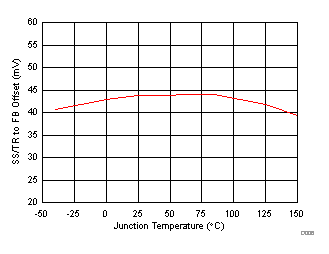
| VSS(ofs) | SS/TR-to-FB matching | V(SS/TR) = 0.4 V | 42 | mV | |||
| SS/TR-to-reference crossover | 98% nominal | 1.16 | V | ||||
| SS/TR discharge current (overload) | V(FB) = 0 V, V(SS/TR) = 0.4 V | 354 | µA | ||||
| SS/TR discharge voltage | V(FB) = 0 V | 54 | mV | ||||
| POWER GOOD (PWRGD PIN) | |||||||
| FB threshold for PWRGD low | FB falling | 90% | |||||
| FB threshold for PWRGD high | FB rising | 93% | |||||
| FB threshold for PWRGD low | FB rising | 108% | |||||
| FB threshold for PWRGD high | FB falling | 106% | |||||
| Hysteresis | FB falling | 2.5% | |||||
| Output high leakage | V(PWRGD) = 5.5 V, TA = 25°C | 10 | nA | ||||
| On resistance | I(PWRGD) = 3 mA, V(FB) < 0.79 V | 45 | Ω | ||||
| Minimum VIN for defined output | V(PWRGD) < 0.5 V, I(PWRGD) = 100 µA | 0.9 | 2 | V | |||
(1) Open Loop current limit measured directly at the SW pin and is independent of the inductor value and slope compensation.
6.6 Timing Requirements
| MIN | TYP | MAX | UNIT | ||
|---|---|---|---|---|---|
| RT/CLK | |||||
| Minimum CLK input pulse width | 15 | ns | |||
6.7 Switching Characteristics
TJ = –40°C to 150°C, V(VIN) = 4.5 V to 60 V (unless otherwise noted)| PARAMETER | TEST CONDITIONS | MIN | TYP | MAX | UNIT | |
|---|---|---|---|---|---|---|
| ENABLE AND UVLO (EN PIN) | ||||||
| Enable to COMP active | V(VIN) = 12 V, TA = 25°C | 540 | µs | |||
| CURRENT-LIMIT | ||||||
| Current limit threshold delay | 60 | ns | ||||
| SW | ||||||
| ton | Minimum on time | V(VIN) = 23.7 V, VO = 5 V, IO = 3.5 A, R(RT) = 39.6 kΩ, TA = 25°C | 100 | ns | ||
| RT/CLK | ||||||
| Switching frequency range using RT mode | 100 | 2500 | kHz | |||
| ƒS | Switching frequency | R(RT) = 200 kΩ | 450 | 500 | 550 | kHz |
| Switching frequency range using CLK mode | 160 | 2300 | kHz | |||
| TIMING RESISTOR AND EXTERNAL CLOCK (RT/CLK PIN) | ||||||
| RT/CLK falling edge to SW rising edge delay | Measured at 500 kHz with an RT resistor (R(RT)) in series | 55 | ns | |||
| PLL lock in time | Measured at 500 kHz | 78 | μs | |||
6.8 Typical Characteristics
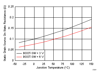
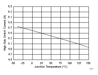
| V(VIN) = 12 V | ||
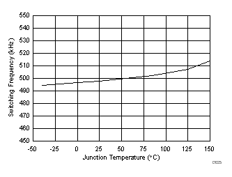
| V(VIN) = 12 V | R(RT) = 200 kΩ | |
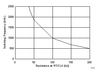
High Frequency Range
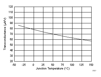
| V(VIN) = 12 V | ||
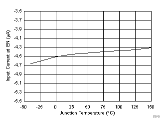
| V(VIN) = 12 V | V(EN) = Threshold + 50 mV | |
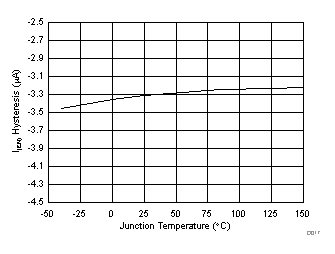
| V(VIN) = 12 V | ||
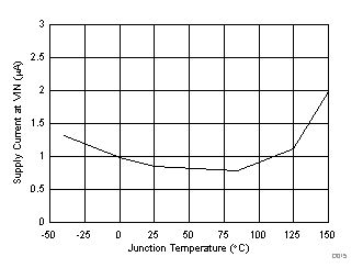
| V(VIN) = 12 V | ||
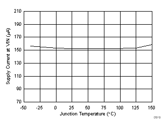
| V(VIN) = 12 V | ||
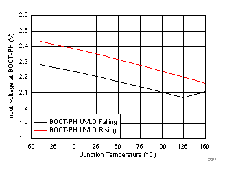
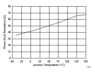
| V(VIN) = 12 V | ||
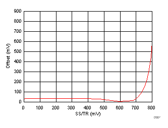
| V(VIN) = 12 V | 25°C | |
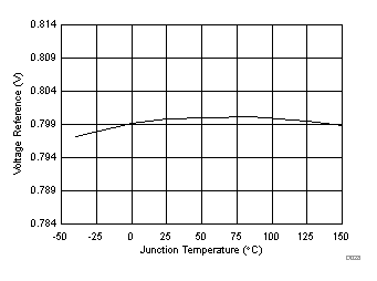
| V(VIN) = 12 V | ||
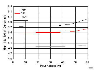
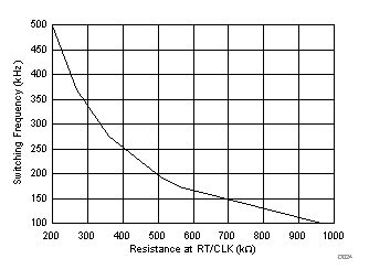
Low Frequency Range
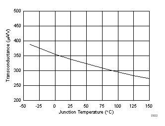
| V(VIN) = 12 V | ||
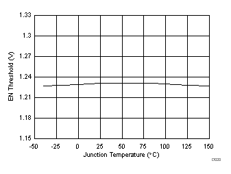
| V(VIN) = 12 V | ||
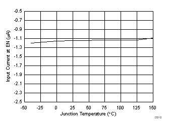
| V(VIN) = 12 V | V(EN) = Threshold – 50 mV | |
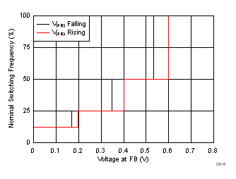
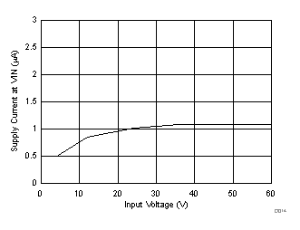
| TJ = 25 °C | ||
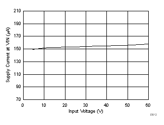
| TJ = 25°C | ||
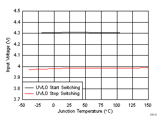
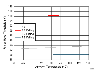
| V(VIN) = 12 V | ||
| V(VIN) = 12 V | V(FB) = 0.4 V | |
