JAJSPW0B June 2023 – June 2024 TPS543B25T
PRODUCTION DATA
- 1
- 1 特長
- 2 アプリケーション
- 3 概要
- 4 Pin Configuration and Functions
- 5 Specifications
-
6 Detailed Description
- 6.1 Overview
- 6.2 Functional Block Diagram
- 6.3
Feature Description
- 6.3.1 VIN Pins and VIN UVLO
- 6.3.2 Internal Linear Regulator and Bypassing
- 6.3.3 Enable and Adjustable UVLO
- 6.3.4 Switching Frequency Selection
- 6.3.5 Switching Frequency Synchronization to an External Clock
- 6.3.6 Remote Sense Amplifier and Adjusting the Output Voltage
- 6.3.7 Loop Compensation Guidelines
- 6.3.8 Soft Start and Prebiased Output Start-Up
- 6.3.9 MSEL Pin
- 6.3.10 Power Good (PG)
- 6.3.11 Output Overload Protection
- 6.3.12 Output Overvoltage and Undervoltage Protection
- 6.3.13 Overtemperature Protection
- 6.3.14 Output Voltage Discharge
- 6.4 Device Functional Modes
-
7 Application and Implementation
- 7.1 Application Information
- 7.2
Typical Applications
- 7.2.1
1.0V Output, 1MHz Application
- 7.2.1.1 Design Requirements
- 7.2.1.2
Detailed Design Procedure
- 7.2.1.2.1 Custom Design With WEBENCH® Tools
- 7.2.1.2.2 Switching Frequency
- 7.2.1.2.3 Output Inductor Selection
- 7.2.1.2.4 Output Capacitor
- 7.2.1.2.5 Input Capacitor
- 7.2.1.2.6 Adjustable Undervoltage Lockout
- 7.2.1.2.7 Output Voltage Resistors Selection
- 7.2.1.2.8 Bootstrap Capacitor Selection
- 7.2.1.2.9 VDRV and VCC Capacitor Selection
- 7.2.1.2.10 PGOOD Pullup Resistor
- 7.2.1.2.11 Current Limit Selection
- 7.2.1.2.12 Soft-Start Time Selection
- 7.2.1.2.13 Ramp Selection and Control Loop Stability
- 7.2.1.2.14 MODE Pin
- 7.2.1.3 Application Curves
- 7.2.1
1.0V Output, 1MHz Application
- 7.3 Power Supply Recommendations
- 7.4 Layout
- 8 Device and Documentation Support
- 9 Revision History
- 10Mechanical, Packaging, and Orderable Information
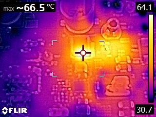
7.4.3 Thermal Performance
Test Conditions: fSW = 1MHz, Vin = 12V, Vout = 1V, Iout = 25A, Inductor = 150nH (0.39mΩ typical), ambient temperature = 25°C
 Figure 7-24 Thermal Image at
25°C Ambient