SLUSC81 May 2015 TPS544B25 , TPS544C25
PRODUCTION DATA.
- 1 Features
- 2 Applications
- 3 Description
- 4 Revision History
- 5 Device Comparison Table
- 6 Pin Configuration and Functions
- 7 Specifications
-
8 Detailed Description
- 8.1 Overview
- 8.2 Functional Block Diagram
- 8.3
Feature Description
- 8.3.1 Linear Regulators BP3 and BP6
- 8.3.2 Input Undervoltage Lockout (UVLO)
- 8.3.3 Turn-On and Turn-Off Delay and Sequencing
- 8.3.4 Voltage Reference
- 8.3.5 Differential Remote Sense
- 8.3.6 Set Output Voltage and Adapative Voltage Scaling (AVS)
- 8.3.7 Reset VOUT
- 8.3.8 Switching Frequency and Synchronization
- 8.3.9 Soft-Start and TON_RISE Command
- 8.3.10 Pre-Biased Output Start-Up
- 8.3.11 Soft-Stop and TOFF_FALL Command
- 8.3.12 Current Monitoring and Low-Side MOSFET Overcurrent Protection
- 8.3.13 High-Side MOSFET Short-Circuit Protection
- 8.3.14 Over-Temperature Protection
- 8.3.15 Output Overvoltage and Undervoltage Protection
- 8.3.16 TON_MAX Fault
- 8.3.17 Power Good (PGOOD) Indicator
- 8.3.18 Fault Protection Responses
- 8.3.19 Switching Node
- 8.3.20 PMBus General Description
- 8.3.21 PMBus Address
- 8.3.22 PMBus Connections
- 8.3.23 Auto ARA (Alert Response Address) Response
- 8.4 Device Functional Modes
- 8.5 Supported PMBus Commands
- 8.6
Register Maps
- 8.6.1 OPERATION (01h)
- 8.6.2 ON_OFF_CONFIG (02h)
- 8.6.3 CLEAR_FAULTS (03h)
- 8.6.4 WRITE_PROTECT (10h)
- 8.6.5 STORE_DEFAULT_ALL (11h)
- 8.6.6 RESTORE_DEFAULT_ALL (12h)
- 8.6.7 CAPABILITY (19h)
- 8.6.8 SMBALERT_MASK (1Bh)
- 8.6.9 VOUT_MODE (20h)
- 8.6.10 VOUT_COMMAND (21h)
- 8.6.11 VOUT_MAX (24h)
- 8.6.12 VOUT_TRANSITION_RATE (27h)
- 8.6.13 VOUT_SCALE_LOOP (29h)
- 8.6.14 VIN_ON (35h)
- 8.6.15 VIN_OFF (36h)
- 8.6.16 IOUT_CAL_OFFSET (39h)
- 8.6.17 VOUT_OV_FAULT_LIMIT (40h)
- 8.6.18 VOUT_OV_FAULT_RESPONSE (41h)
- 8.6.19 VOUT_OV_WARN_LIMIT (42h)
- 8.6.20 VOUT_UV_WARN_LIMIT (43h)
- 8.6.21 VOUT_UV_FAULT_LIMIT (44h)
- 8.6.22 VOUT_UV_FAULT_RESPONSE (45h)
- 8.6.23 IOUT_OC_FAULT_LIMIT (46h)
- 8.6.24 IOUT_OC_FAULT_RESPONSE (47h)
- 8.6.25 IOUT_OC_WARN_LIMIT (4Ah)
- 8.6.26 OT_FAULT_LIMIT (4Fh)
- 8.6.27 OT_FAULT_RESPONSE (50h)
- 8.6.28 OT_WARN_LIMIT (51h)
- 8.6.29 TON_DELAY (60h)
- 8.6.30 TON_RISE (61h)
- 8.6.31 TON_MAX_FAULT_LIMIT (62h)
- 8.6.32 TON_MAX_FAULT_RESPONSE (63h)
- 8.6.33 TOFF_DELAY (64h)
- 8.6.34 TOFF_FALL (65h)
- 8.6.35 STATUS_BYTE (78h)
- 8.6.36 STATUS_WORD (79h)
- 8.6.37 STATUS_VOUT (7Ah)
- 8.6.38 STATUS_IOUT (7Bh)
- 8.6.39 STATUS_INPUT (7Ch)
- 8.6.40 STATUS_TEMPERATURE (7Dh)
- 8.6.41 STATUS_CML (7Eh)
- 8.6.42 STATUS_MFR_SPECIFIC (80h)
- 8.6.43 READ_VOUT (8Bh)
- 8.6.44 READ_IOUT (8Ch)
- 8.6.45 READ_TEMPERATURE_2 (8Eh)
- 8.6.46 PMBUS_REVISION (98h)
- 8.6.47 MFR_VOUT_MIN (A4h)
- 8.6.48 IC_DEVICE_ID (ADh)
- 8.6.49 IC_DEVICE_REV (AEh)
- 8.6.50 MFR_SPECIFIC_00 (D0h)
- 8.6.51 OPTIONS (MFR_SPECIFIC_21) (E5h)
- 8.6.52 MISC_CONFIG_OPTIONS (MFR_SPECIFIC_32) (F0h)
-
9 Applications and Implementation
- 9.1 Application Information
- 9.2
Typical Applications
- 9.2.1 TPS544C25 4.5-V to 18-V Input, 0.95-V Output, 30-A Converter
- 9.2.2 Design Requirements
- 9.2.3
Design Procedure
- 9.2.3.1 Switching Frequency Selection
- 9.2.3.2 Inductor Selection
- 9.2.3.3 Output Capacitor Selection
- 9.2.3.4 Input Capacitor Selection
- 9.2.3.5 Bootstrap Capacitor Selection
- 9.2.3.6 BP6 and BP3
- 9.2.3.7 R-C Snubber and VIN Pin High-Frequency Bypass
- 9.2.3.8 Temperature Sensor
- 9.2.3.9 Key PMBus Parameter Selection
- 9.2.3.10 Output Voltage Setting and Frequency Compensation Selection
- 9.2.4 Application Curves
- 10Power Supply Recommendations
- 11Layout
- 12Device and Documentation Support
- 13Mechanical, Packaging, and Orderable Information
パッケージ・オプション
メカニカル・データ(パッケージ|ピン)
- RVF|40
サーマルパッド・メカニカル・データ
- RVF|40
発注情報
11 Layout
11.1 Layout Guidelines
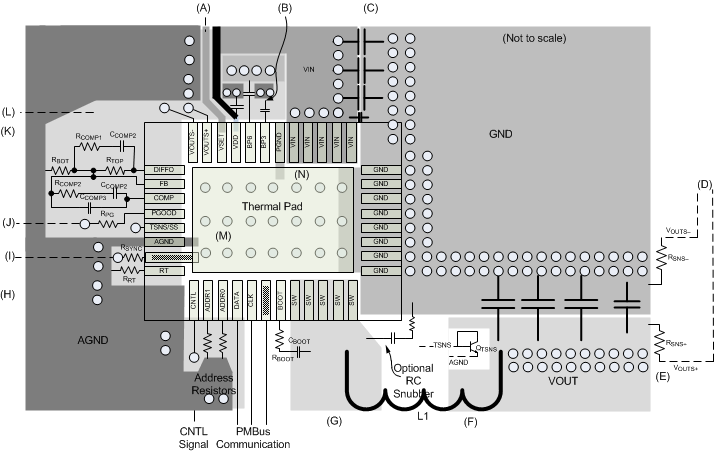
Layout is a critical portion of good power supply design. Figure 55 shows the recommended PCB layout configuration. A list of PCB layout considerations using these devices are listed below.
- As with any switching regulator, there are several signal paths that conduct fast switching voltages or currents. Minimize the loop area formed by these paths and their bypass connections.
- Bypass the VIN pins to GND with a low-impedance path. Power-stage input bypass capacitors should be as close as physically possible to the VIN and GND pins. Additionally, a high-frequency bypass capacitor in 0402 package on the VIN pins can help to reduce switching spikes, which can be tucked right underneath the IC on the other side of the PCB to keep a minimum loop.
- BP6 bypass capacitor carries large switching current for gate driver. Bypassing the BP6 pin to GND with a low-impedance path is very critical to the stable operation of the TPS544x25 devices. Place BP6 high-frequency bypass capacitors as close as possible to the device pins, with a minimum return loop back to ground.
- The VDD and BP3 also require good local bypassing. Place bypass capacitors as close as possible to the device pins, with a minimum return loop back to ground and this return loop should be kept away from fast switching voltage and main current path, as well as BP6 current path. Poor bypassing on VDD and BP3 can degrade the performance of the regulator.
- Keep signal components local to the device, and place them as close as possible to the pins to which they are connected. These components include the feedback resistors, the RT resistor, the VSET resistor, the SS resistor, as well as ADDR0 and ADDR1 resistors. These components should also be kept away from fast switching voltage and current paths. Those components can be terminated to GND with minimum return loop or bypassed to a separate low impedance analog ground (AGND) copper area, which is isolated from fast switching voltage and current paths and has single connection to PGND on the thermal tab via AGND pin. See Figure 55 for placement recommendation.
- The PGND pin (pin 26) must be directly connected to the thermal pad of the device on the PCB, with a low-noise, low-impedance path to ensure accurate current monitoring.
- Minimize the SW copper area for best noise performance. Route sensitive traces away from SW and BOOT, as these nets contain fast switching voltages, and lend easily to capacitive coupling.
- Snubber component placement is critical to its effectiveness of ringing reduction. These components should be on the same layer as the TPS544x25 devices, and be kept as close as possible to the SW and GND copper areas.
- The VIN and VDD pins must be the same potential for accurate short circuit protection, but high frequency switching noise on the VDD pin can degrade performance. VDD should be connected to VIN through a trace from the input copper area. Optionally form a small low-pass R-C between VIN and VDD, with the VDD bypass capacitor (1 µF) and a 0-2 Ω resistor between VIN and VDD. See Figure 55.
- Route the VOUTS+ and VOUTS– lines from the output capacitor bank at the load back to the device pins as a tightly coupled differential pair. It is critical that these traces be kept away from switching or noisy areas which can add differential-mode noise.
- Routing of the temperature sensor traces is critical to the noise performance of temperature monitoring. Keep these traces away from switching areas or high current paths on the layout. It is also recommended to use a small 1-nF capacitor from TSNS/SS to AGND to improve the noise performance of temperature readings.
11.2 Layout Example

(A) Connect to AGND with setting resistor or pull up to BP3 if not used.
(B) Bypass for internal regulators BP3, BP6, VDD. Use multiple vias to reduce parasitic inductance
(C) Place VIN bypass capacitors as close as possible to device, with best high frequency capacitor closest to VIN and GND pins
(D) Kelvin connect to TPS544C25 VOUTS– and VOUTS+ pins
(E) Sense point should be directly at the load
(F) For best efficiency, use a heavy weight copper and place these planes on multiple PCB layers
(G) Minimize SW area for least noise. Keep sensitive traces away from SW and BOOT on all layers
(H) AGND and PGND are only connected together on Thermal Pad.
(I) Optional SYNC/RESET_B Signal. Pull up to BP3 if not used.
(J) Pull up to BP6 or external voltage to use PGOOD.
(K) Maintain feedback and compensation network components localized to the device.
(L) Internal AGND Plane to reduce the BP3 and VDD bypass parasitics.
(M) Connect AGND to Thermal Pad
(N) Connect PGND to Thermal Pad
Figure 55. PCB Layout Recommendation
(B) Bypass for internal regulators BP3, BP6, VDD. Use multiple vias to reduce parasitic inductance
(C) Place VIN bypass capacitors as close as possible to device, with best high frequency capacitor closest to VIN and GND pins
(D) Kelvin connect to TPS544C25 VOUTS– and VOUTS+ pins
(E) Sense point should be directly at the load
(F) For best efficiency, use a heavy weight copper and place these planes on multiple PCB layers
(G) Minimize SW area for least noise. Keep sensitive traces away from SW and BOOT on all layers
(H) AGND and PGND are only connected together on Thermal Pad.
(I) Optional SYNC/RESET_B Signal. Pull up to BP3 if not used.
(J) Pull up to BP6 or external voltage to use PGOOD.
(K) Maintain feedback and compensation network components localized to the device.
(L) Internal AGND Plane to reduce the BP3 and VDD bypass parasitics.
(M) Connect AGND to Thermal Pad
(N) Connect PGND to Thermal Pad
11.2.1 Mounting and Thermal Profile Recommendation
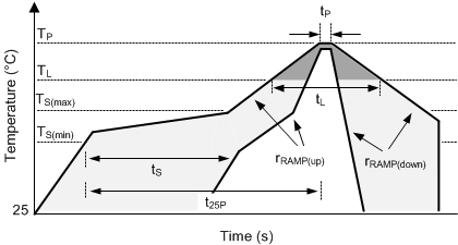
Proper mounting technique adequately covers the exposed thermal tab with solder. Excessive heat during the reflow process can affect electrical performance. Figure 56 shows the recommended reflow oven thermal profile. Proper post-assembly cleaning is also critical to device performance. See SLUA271 for more information.
 Figure 56. Recommended Reflow Oven Thermal Profile
Table 18. Recommended Thermal Profile Parameters
| PARAMETER | MIN | TYP | MAX | UNIT | |
|---|---|---|---|---|---|
| RAMP UP AND RAMP DOWN | |||||
| rRAMP(up) | Average ramp-up rate, TS(max) to TP | 3 | °C/s | ||
| rRAMP(down) | Average ramp-down rate, TP to TS(max) | 6 | °C/s | ||
| PRE-HEAT | |||||
| TS | Pre-heat temperature | 150 | 200 | °C | |
| tS | Pre-heat time, TS(min) to TS(max) | 60 | 180 | s | |
| REFLOW | |||||
| TL | Liquidus temperature | 217 | °C | ||
| TP | Peak temperature | 260 | °C | ||
| tL | Time maintained above liquidus temperature, TL | 60 | 150 | s | |
| tP | Time maintained within 5 °C of peak temperature, TP | 20 | 40 | s | |
| t25P | Total time from 25 °C to peak temperature, TP | 480 | s | ||