JAJSLN5B May   2012  – April 2021 TPS54525

PRODUCTION DATA  

  1. 特長
  2. アプリケーション
  3. 概要
  4. Revision History
  5. Pin Configuration and Functions
  6. Specifications
    1. 6.1 Absolute Maximum Ratings
    2. 6.2 ESD Ratings
    3. 6.3 Recommended Operating Conditions
    4. 6.4 Thermal Information
    5. 6.5 Electrical Characteristics
    6. 6.6 Typical Characteristics
  7. Detailed Description
    1. 7.1 Overview
    2. 7.2 Functional Block Diagram
    3. 7.3 Feature Description
      1. 7.3.1  PWM Operation
      2. 7.3.2  PWM Frequency and Adaptive On-Time Control
      3. 7.3.3  Soft Start and Pre-Biased Soft Start
      4. 7.3.4  Power Good
      5. 7.3.5  VREG5
      6. 7.3.6  Output Discharge Control
      7. 7.3.7  Current Protection
      8. 7.3.8  Over/Under Voltage Protection
      9. 7.3.9  UVLO Protection
      10. 7.3.10 Thermal Shutdown
    4. 7.4 Device Functional Modes
      1. 7.4.1 Forced CCM Mode
  8. Application and Implementation
    1. 8.1 Application Information
    2. 8.2 Typical Application
      1. 8.2.1 Design Requirements
      2. 8.2.2 Detailed Design Procedure
        1. 8.2.2.1 Step By Step Design Procedure
        2. 8.2.2.2 Output Voltage Resistors Selection
        3. 8.2.2.3 Output Filter Selection
        4. 8.2.2.4 Input Capacitor Selection
        5. 8.2.2.5 Bootstrap Capacitor Selection
        6. 8.2.2.6 VREG5 Capacitor Selection
      3. 8.2.3 Application Curves
  9. Power Supply Recommendations
  10. 10Layout
    1. 10.1 Layout Guidelines
    2. 10.2 Layout Guidelines
      1. 10.2.1 Thermal Considerations
  11. 11Device and Documentation Support
    1. 11.1 Device Support
      1. 11.1.1 Third-Party Products Disclaimer
    2. 11.2 Receiving Notification of Documentation Updates
    3. 11.3 サポート・リソース
    4. 11.4 Trademarks
    5. 11.5 静電気放電に関する注意事項
    6. 11.6 用語集

パッケージ・オプション

メカニカル・データ(パッケージ|ピン)
サーマルパッド・メカニカル・データ
発注情報

Soft Start and Pre-Biased Soft Start

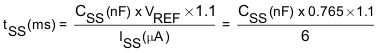
The soft start function is adjustable. When the EN pin becomes high, 6-μA current begins charging the capacitor which is connected from the SS pin to GND. Smooth control of the output voltage is maintained during start up. The equation for the slow start time is shown in Equation 1. VFB voltage is 0.765 V and SS pin source current is 6 μA.

Equation 1. GUID-05924323-D0A8-4A32-97CD-A777A4FA29D0-low.gif

The TPS54525 contains a unique circuit to prevent current from being pulled from the output during startup if the output is pre-biased. When the soft-start commands a voltage higher than the pre-bias level (internal soft start becomes greater than feedback voltage VFB), the controller slowly activates synchronous rectification by starting the first low side FET gate driver pulses with a narrow on-time. It then increments that on-time on a cycle-by-cycle basis until it coincides with the time dictated by (1-D), where D is the duty cycle of the converter. This scheme prevents the initial sinking of the pre-bias output, and ensure that the out voltage (VO) starts and ramps up smoothly into regulation and the control loop is given time to transition from pre-biased start-up to normal mode operation.