JAJSBM7C September 2011 – October 2017 TPS54623
PRODUCTION DATA.
- 1 特長
- 2 アプリケーション
- 3 概要
- 4 改訂履歴
- 5 Pin Configuration and Functions
- 6 Specifications
-
7 Detailed Description
- 7.1 Overview
- 7.2 Functional Block Diagram
- 7.3
Feature Description
- 7.3.1 VIN and Power VIN Pins (VIN and PVIN)
- 7.3.2 Voltage Reference
- 7.3.3 Adjusting the Output Voltage
- 7.3.4 Safe Start-up into Pre-Biased Outputs
- 7.3.5 Error Amplifier
- 7.3.6 Slope Compensation
- 7.3.7 Enable and Adjusting Undervoltage Lockout
- 7.3.8 Slow Start (SS/TR)
- 7.3.9 Power Good (PWRGD)
- 7.3.10 Bootstrap Voltage (BOOT) and Low Dropout Operation
- 7.3.11 Sequencing (SS/TR)
- 7.3.12 Output Overvoltage Protection (OVP)
- 7.3.13 Overcurrent Protection
- 7.3.14 Thermal Shutdown
- 7.3.15 Small Signal Model for Loop Response
- 7.3.16 Simple Small Signal Model for Peak Current Mode Control
- 7.3.17 Small Signal Model for Frequency Compensation
- 7.4 Device Functional Modes
-
8 Application and Implementation
- 8.1 Application Information
- 8.2
Typical Application
- 8.2.1 Design Requirements
- 8.2.2
Detailed Design Procedure
- 8.2.2.1 Custom Design With WEBENCH® Tools
- 8.2.2.2 Operating Frequency
- 8.2.2.3 Output Inductor Selection
- 8.2.2.4 Output Capacitor Selection
- 8.2.2.5 Input Capacitor Selection
- 8.2.2.6 Slow Start Capacitor Selection
- 8.2.2.7 Bootstrap Capacitor Selection
- 8.2.2.8 Under Voltage Lockout Set Point
- 8.2.2.9 Output Voltage Feedback Resistor Selection
- 8.2.2.10 Compensation Component Selection
- 8.2.3 Application Curves
- 9 Power Supply Recommendations
- 10Layout
- 11デバイスおよびドキュメントのサポート
- 12メカニカル、パッケージ、および注文情報
6.6 Typical Characteristics
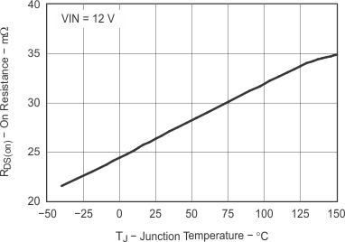 Figure 1. High-Side RDS(on) vs Temperature
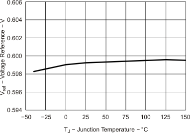 Figure 3. Voltage Reference vs Temperature
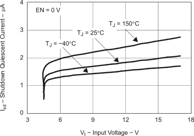 Figure 5. Shutdown Quiescent Current
vs Input Voltage
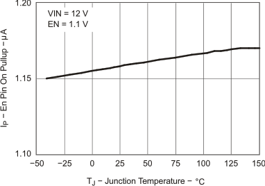 Figure 7. Pin Pullup Current vs Temperature
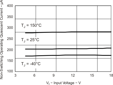 Figure 9. Non-Switching Operating Quiescent
Current (VIN) vs Input Voltage
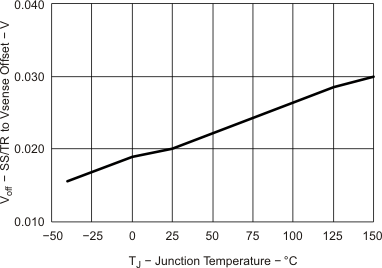 Figure 11. (SS/TR - VSENSE) Offset vs Temperature
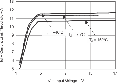 Figure 13. High-Side Current limit Threshold
vs Input Voltage
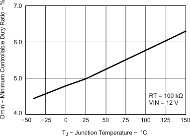 Figure 15. Minimum Controllable Duty Ratio
vs Junction Temperature
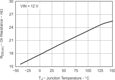 Figure 2. Low-Side RDS(on) vs Temperature
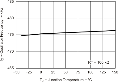 Figure 4. Oscillator Frequency vs Temperature
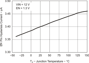 Figure 6. EN Pin Hysteresis Current vs Temperature
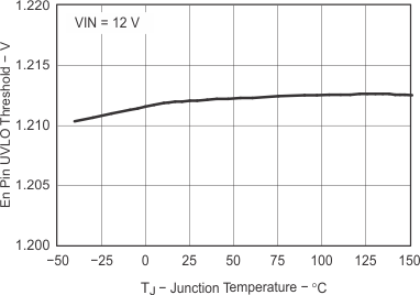 Figure 8. Pin UVLO Threshold vs Temperature
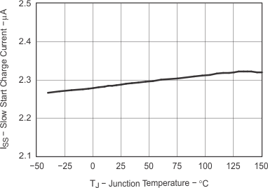 Figure 10. Slow Start Charge Current
vs Temperature
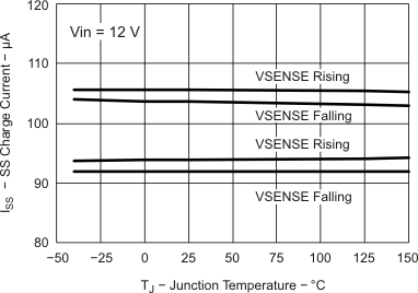 Figure 12. PWRGD Threshold vs Temperature
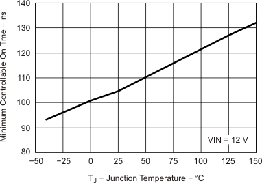 Figure 14. Minimum Controllable On Time
vs Temperature
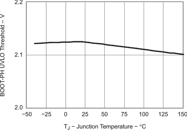 Figure 16. BOOT-PH UVLO Threshold
vs Temperature