JAJSBM7C September 2011 – October 2017 TPS54623
PRODUCTION DATA.
- 1 特長
- 2 アプリケーション
- 3 概要
- 4 改訂履歴
- 5 Pin Configuration and Functions
- 6 Specifications
-
7 Detailed Description
- 7.1 Overview
- 7.2 Functional Block Diagram
- 7.3
Feature Description
- 7.3.1 VIN and Power VIN Pins (VIN and PVIN)
- 7.3.2 Voltage Reference
- 7.3.3 Adjusting the Output Voltage
- 7.3.4 Safe Start-up into Pre-Biased Outputs
- 7.3.5 Error Amplifier
- 7.3.6 Slope Compensation
- 7.3.7 Enable and Adjusting Undervoltage Lockout
- 7.3.8 Slow Start (SS/TR)
- 7.3.9 Power Good (PWRGD)
- 7.3.10 Bootstrap Voltage (BOOT) and Low Dropout Operation
- 7.3.11 Sequencing (SS/TR)
- 7.3.12 Output Overvoltage Protection (OVP)
- 7.3.13 Overcurrent Protection
- 7.3.14 Thermal Shutdown
- 7.3.15 Small Signal Model for Loop Response
- 7.3.16 Simple Small Signal Model for Peak Current Mode Control
- 7.3.17 Small Signal Model for Frequency Compensation
- 7.4 Device Functional Modes
-
8 Application and Implementation
- 8.1 Application Information
- 8.2
Typical Application
- 8.2.1 Design Requirements
- 8.2.2
Detailed Design Procedure
- 8.2.2.1 Custom Design With WEBENCH® Tools
- 8.2.2.2 Operating Frequency
- 8.2.2.3 Output Inductor Selection
- 8.2.2.4 Output Capacitor Selection
- 8.2.2.5 Input Capacitor Selection
- 8.2.2.6 Slow Start Capacitor Selection
- 8.2.2.7 Bootstrap Capacitor Selection
- 8.2.2.8 Under Voltage Lockout Set Point
- 8.2.2.9 Output Voltage Feedback Resistor Selection
- 8.2.2.10 Compensation Component Selection
- 8.2.3 Application Curves
- 9 Power Supply Recommendations
- 10Layout
- 11デバイスおよびドキュメントのサポート
- 12メカニカル、パッケージ、および注文情報
7.4.3 Light Load Efficiency Operation
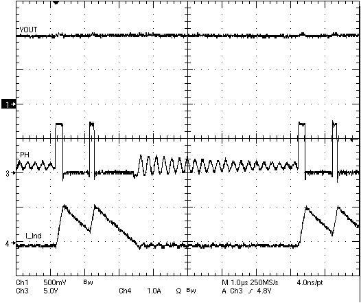
The TPS54623 operates in pulse skip mode (see Figure 28) at light load currents to improve efficiency by reducing switching and gate drive losses. The TPS54623 is designed so that if the output voltage is within regulation and the peak switch current at the end of any switching cycle is below the pulse skipping current threshold, the device enters pulse skip mode. This current threshold is the current level corresponding to a nominal COMP voltage of 250 mV.
When in pulse skip mode, the COMP pin voltage is clamped and the high side MOSFET is inhibited. Further decreases in load current or in output voltage can not drive the COMP pin below this clamp voltage level.
Since the device is not switching, the output voltage begins to decay. As the voltage control loop compensates for the falling output voltage, the COMP pin voltage begins to rise. At this time, the high side MOSFET is enabled and a switching pulse initiates on the next switching cycle. The peak current is set by the COMP pin voltage. The output voltage re-charges the regulated value, then the peak switch current starts to decrease, and eventually falls below the pulse skip mode threshold at which time the device again enters pulse skip mode.
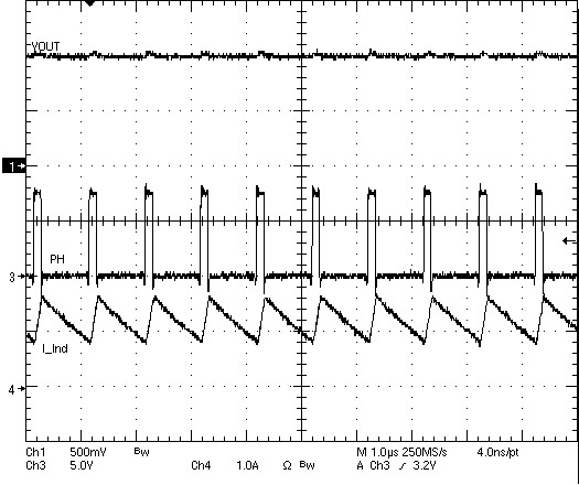
 Figure 27. TPS54623 Operation In Current Mode
 Figure 28. TPS54623 Operation In Pulse Skipping Mode