JAJSBM7C September 2011 – October 2017 TPS54623
PRODUCTION DATA.
- 1 特長
- 2 アプリケーション
- 3 概要
- 4 改訂履歴
- 5 Pin Configuration and Functions
- 6 Specifications
-
7 Detailed Description
- 7.1 Overview
- 7.2 Functional Block Diagram
- 7.3
Feature Description
- 7.3.1 VIN and Power VIN Pins (VIN and PVIN)
- 7.3.2 Voltage Reference
- 7.3.3 Adjusting the Output Voltage
- 7.3.4 Safe Start-up into Pre-Biased Outputs
- 7.3.5 Error Amplifier
- 7.3.6 Slope Compensation
- 7.3.7 Enable and Adjusting Undervoltage Lockout
- 7.3.8 Slow Start (SS/TR)
- 7.3.9 Power Good (PWRGD)
- 7.3.10 Bootstrap Voltage (BOOT) and Low Dropout Operation
- 7.3.11 Sequencing (SS/TR)
- 7.3.12 Output Overvoltage Protection (OVP)
- 7.3.13 Overcurrent Protection
- 7.3.14 Thermal Shutdown
- 7.3.15 Small Signal Model for Loop Response
- 7.3.16 Simple Small Signal Model for Peak Current Mode Control
- 7.3.17 Small Signal Model for Frequency Compensation
- 7.4 Device Functional Modes
-
8 Application and Implementation
- 8.1 Application Information
- 8.2
Typical Application
- 8.2.1 Design Requirements
- 8.2.2
Detailed Design Procedure
- 8.2.2.1 Custom Design With WEBENCH® Tools
- 8.2.2.2 Operating Frequency
- 8.2.2.3 Output Inductor Selection
- 8.2.2.4 Output Capacitor Selection
- 8.2.2.5 Input Capacitor Selection
- 8.2.2.6 Slow Start Capacitor Selection
- 8.2.2.7 Bootstrap Capacitor Selection
- 8.2.2.8 Under Voltage Lockout Set Point
- 8.2.2.9 Output Voltage Feedback Resistor Selection
- 8.2.2.10 Compensation Component Selection
- 8.2.3 Application Curves
- 9 Power Supply Recommendations
- 10Layout
- 11デバイスおよびドキュメントのサポート
- 12メカニカル、パッケージ、および注文情報
8.2.3 Application Curves
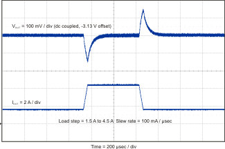 Figure 32. Load Transient
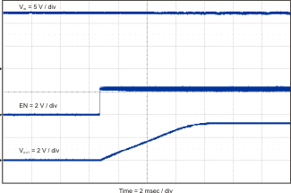 Figure 34. Startup with EN
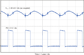 Figure 36. Output Voltage Ripple With Full Load
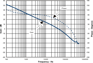 Figure 38. Closed Loop Response
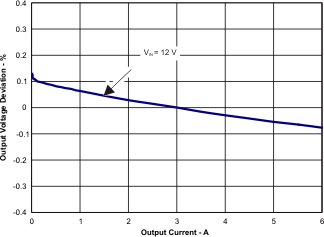 Figure 40. Load Regulation
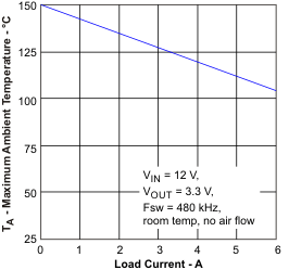 Figure 42. Maximum Ambient Temperature
vs Load Current
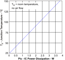 Figure 44. Junction Temperature
vs IC Power Dissipation
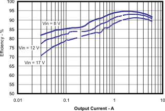 Figure 46. Efficiency vs Output Current
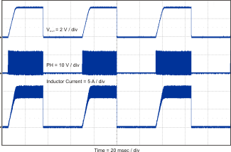
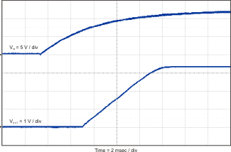 Figure 33. Start-Up With VIN
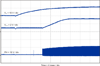 Figure 35. Start-Up With Pre-Bias
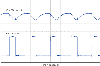 Figure 37. Input Voltage Ripple with Full Load
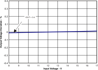 Figure 39. Line Regulation
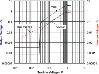 Figure 41. Tracking Performance
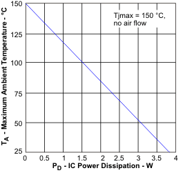 Figure 43. Maximum Ambient Temperature
vs IC Power Dissipation
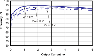 Figure 45. Efficiency vs Load Current
