JAJSIT5D March 2020 – July 2021 TPS548A29
PRODUCTION DATA
- 1 特長
- 2 アプリケーション
- 3 概要
- 4 Revision History
- 5 Pin Configuration and Functions
- 6 Specifications
-
7 Detailed Description
- 7.1 Overview
- 7.2 Functional Block Diagram
- 7.3
Feature Description
- 7.3.1 Internal VCC LDO And Using External Bias On VCC Pin
- 7.3.2 Enable
- 7.3.3 Output Voltage Setting
- 7.3.4 Internal Fixed Soft Start and External Adjustable Soft Start
- 7.3.5 External REFIN For Output Voltage Tracking
- 7.3.6 Frequency and Operation Mode Selection
- 7.3.7 D-CAP3 Control
- 7.3.8 Low-side FET Zero-Crossing
- 7.3.9 Current Sense and Positive Overcurrent Protection
- 7.3.10 Low-side FET Negative Current Limit
- 7.3.11 Power Good
- 7.3.12 Overvoltage and Undervoltage Protection
- 7.3.13 Out-Of-Bounds (OOB) Operation
- 7.3.14 Output Voltage Discharge
- 7.3.15 UVLO Protection
- 7.3.16 Thermal Shutdown
- 7.4 Device Functional Modes
-
8 Application and Implementation
- 8.1 Application Information
- 8.2
Typical Application
- 8.2.1 Design Requirements
- 8.2.2
Detailed Design Procedure
- 8.2.2.1 Output Voltage Setting Point
- 8.2.2.2 Choose the Switching Frequency and the Operation Mode
- 8.2.2.3 Choose the Inductor
- 8.2.2.4 Set the Current Limit (TRIP)
- 8.2.2.5 Choose the Output Capacitor
- 8.2.2.6 Choose the Input Capacitors (CIN)
- 8.2.2.7 Soft Start Capacitor (SS/REFIN Pin)
- 8.2.2.8 EN Pin Resistor Divider
- 8.2.2.9 VCC Bypass Capacitor
- 8.2.2.10 BOOT Capacitor
- 8.2.2.11 PGOOD Pullup Resistor
- 8.2.3 Application Curves
- 9 Power Supply Recommendations
- 10Layout
- 11Device and Documentation Support
- 12Mechanical, Packaging, and Orderable Information
5 Pin Configuration and Functions
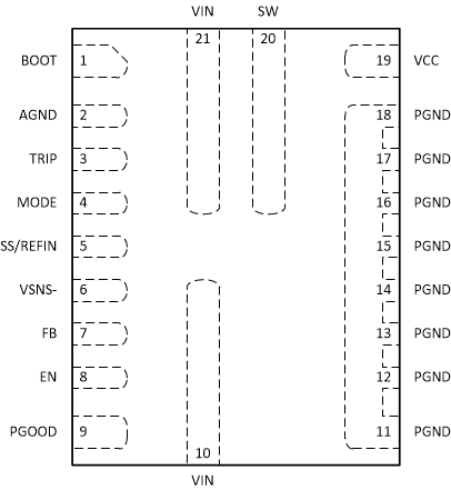
 Figure 5-1 RWW Package21-Pin VQFN-HRTop View
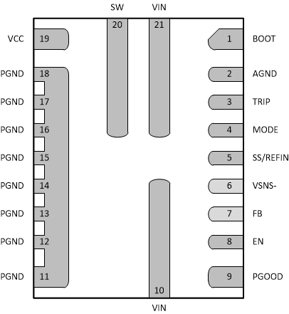
 Figure 5-2 RWW Package21-Pin VQFN-HRBottom
View
Figure 5-2 RWW Package21-Pin VQFN-HRBottom
ViewTable 5-1 Pin Functions
| NO. | NAME | I/O(1) | DESCRIPTION |
|---|---|---|---|
| 1 | BOOT | I/O | Supply rail for the high-side gate driver (boost terminal). Connect the bootstrap capacitor from this pin to SW node. |
| 2 | AGND | G | Ground pin, reference point for the internal control circuits |
| 3 | TRIP | I/O | Current limit setting pin. Connect a resistor to AGND to set the current limit trip point. A ±1% tolerance resistor is highly recommended. See Section 7.3.9 for details on OCL setting. |
| 4 | MODE | I | The MODE pin sets the forced continuous-conduction mode (FCCM) or Skip-mode operation. It also selects the operating frequency by connecting a resistor from the MODE pin to the AGND pin. ±1% tolerance resistor is recommended. See Table 7-1 for details. |
| 5 | SS/REFIN | I/O | Dual-function pin. Soft-start function: Connecting a capacitor to
VSNS– pin programs soft-start time. Minimum soft-start time (1.5 ms)
is fixed internally. A minimum 1-nF capacitor is required for this
pin to avoid overshoot during the charge of soft-start capacitor.
REFIN function: The device always looks at the voltage on this SS/REFIN pin as the reference for the control loop. The internal reference voltage can be overridden by an external DC voltage source on this pin for tracking application. |
| 6 | VSNS– | I | The return connection for a remote voltage sensing configuration. It is also used as ground for the internal reference. Short to AGND for single-end sense configuration. |
| 7 | FB | I | Output voltage feedback input. A resistor divider from the VOUT to VSNS– (tapped to FB pin) sets the output voltage. |
| 8 | EN | I | Enable pin. The enable pin turns the DC/DC switching converter on or off. Floating EN pin before start-up disables the converter. The recommended operating condition for EN pin is maximum 5.5 V. Do not connect EN pin to VIN pin directly. |
| 9 | PGOOD | O | Open-drain power-good status signal. When the FB voltage moves outside the specified limits, PGOOD goes low after 2-µs delay. |
| 10, 21 | VIN | P | Power-supply input pins for both integrated power MOSFET pair and the internal LDO. Place the decoupling input capacitors from VIN pins to PGND pins as close as possible. |
| 11, 12, 13, 14, 15, 16, 17, 18 | PGND | G | Power ground of internal low-side MOSFET. At least six PGND vias are required to be placed as close as possible to the PGND pins. This minimizes parasitic impedance and also lowers thermal resistance. |
| 19 | VCC | I/O | Internal 4.5-V LDO output. An external bias with 5.0-V can be connected to this pin to save the power losses on the internal LDO. The voltage source on this pin powers both the internal circuitry and gate driver. Requires a 2.2-µF, at least 6.3-V rating ceramic capacitor from the VCC pin to PGND pins as the decoupling capacitor and the placement is required to be as close as possible. |
| 20 | SW | O | Output switching terminal of the power converter. Connect this pin to the output inductor. |
(1) I = Input, O = Output, P = Supply, G = Ground