JAJSJZ4B October   2020  – June 2024 TPS54J061

PRODUCTION DATA  

  1.   1
  2. 特長
  3. アプリケーション
  4. 概要
  5. Pin Configuration and Functions
  6. Specifications
    1. 5.1 Absolute Maximum Ratings
    2. 5.2 ESD Ratings
    3. 5.3 Recommended Operating Conditions
    4. 5.4 Thermal Information
    5. 5.5 Electrical Characteristics
    6. 5.6 Typical Characteristics
  7. Detailed Description
    1. 6.1 Overview
    2. 6.2 Functional Block Diagram
    3. 6.3 Feature Description
      1. 6.3.1  Enable and Internal LDO
      2. 6.3.2  Split Rail and External LDO
      3. 6.3.3  Output Voltage Setting
      4. 6.3.4  Soft Start and Output-Voltage Tracking
      5. 6.3.5  Frequency and Operation Mode Selection
      6. 6.3.6  D-CAP3™ Control Mode
      7. 6.3.7  Current Sense and Positive Overcurrent Protection
      8. 6.3.8  Low-side FET Negative Current Limit
      9. 6.3.9  Power Good
      10. 6.3.10 Overvoltage and Undervoltage Protection
      11. 6.3.11 Out-Of-Bounds Operation (OOB)
      12. 6.3.12 Output Voltage Discharge
      13. 6.3.13 UVLO Protection
      14. 6.3.14 Thermal Shutdown
    4. 6.4 Device Functional Modes
      1. 6.4.1 Auto-Skip Eco-Mode Light Load Operation
      2. 6.4.2 Forced Continuous-Conduction Mode
      3. 6.4.3 Pre-Bias Start-up
  8. Application and Implementation
    1. 7.1 Application Information
    2. 7.2 Typical Application
      1. 7.2.1 Design Requirements
      2. 7.2.2 Detailed Design Procedure
        1. 7.2.2.1  Choose the Switching Frequency and Operation Mode (MODE Pin)
        2. 7.2.2.2  Choose the Output Inductor (L)
        3. 7.2.2.3  Set the Current Limit (TRIP)
        4. 7.2.2.4  Choose the Output Capacitors (COUT)
        5. 7.2.2.5  Choose the Input Capacitors (CIN)
        6. 7.2.2.6  Feedback Network (FB Pin)
        7. 7.2.2.7  Soft Start Capacitor (SS/REFIN Pin)
        8. 7.2.2.8  EN Pin Resistor Divider
        9. 7.2.2.9  VCC Bypass Capacitor
        10. 7.2.2.10 BOOT Capacitor
        11. 7.2.2.11 Series BOOT Resistor and RC Snubber
        12. 7.2.2.12 PGOOD Pullup Resistor
      3. 7.2.3 Application Curves
    3. 7.3 Power Supply Recommendations
    4. 7.4 Layout
      1. 7.4.1 Layout Guidelines
      2. 7.4.2 Layout Example
  9. Device and Documentation Support
    1. 8.1 Documentation Support
      1. 8.1.1 Related Documentation
    2. 8.2 サポート・リソース
    3. 8.3 ドキュメントの更新通知を受け取る方法
    4. 8.4 Trademarks
    5. 8.5 用語集
    6. 8.6 静電気放電に関する注意事項
  10. Revision History
  11. 10Mechanical, Packaging, and Ordering Information

パッケージ・オプション

メカニカル・データ(パッケージ|ピン)
サーマルパッド・メカニカル・データ
発注情報

Application Curves

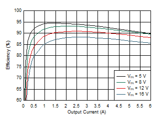
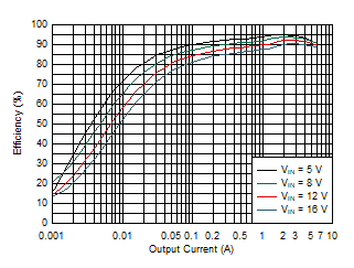
TPS54J061 Efficiency –
            1100 kHz, FCCM
VOUT = 1.8 V fSW = 1100 kHz MODE = FCCM
VCC = Int 3.0 V
Figure 7-2 Efficiency – 1100 kHz, FCCM
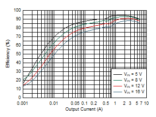
TPS54J061 Efficiency –
            1100 kHz, FCCM, External 3.3-V VCC, 4.7-Ω RBOOT
VOUT = 1.8 V fSW = 1100 kHz MODE = FCCM
VCC = Ext 3.3 V RBOOT = 4.7 Ω
Figure 7-4 Efficiency – 1100 kHz, FCCM, External 3.3-V VCC, 4.7-Ω RBOOT
TPS54J061 Efficiency –
            1100 kHz, DCM, External 3.3-V VCC, 4.7-Ω RBOOT
VOUT = 1.8 V fSW = 1100 kHz MODE = DCM
VCC = Ext 3.3 V RBOOT = 4.7 Ω
Figure 7-6 Efficiency – 1100 kHz, DCM, External 3.3-V VCC, 4.7-Ω RBOOT
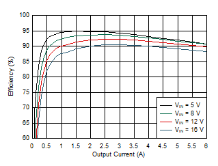
TPS54J061 Efficiency –
            600 kHz, FCCM
VOUT = 1.8 V fSW = 600 kHz MODE = FCCM
VCC = Int 3.0 V
Figure 7-8 Efficiency – 600 kHz, FCCM
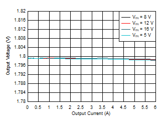
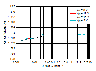
TPS54J061 Output Voltage
            vs Output Current – FCCM
VOUT = 1.8 V fSW = 1100 kHz MODE = FCCM
Figure 7-10 Output Voltage vs Output Current – FCCM
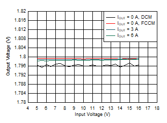
TPS54J061 Output Voltage
            vs Input Voltage
VOUT = 1.8 V fSW = 1100 kHz
Figure 7-12 Output Voltage vs Input Voltage
TPS54J061 Switching
            Frequency vs Output Current – 600 kHz
VOUT = 1.8 V fSW = 600 kHz MODE = FCCM
Figure 7-14 Switching Frequency vs Output Current – 600 kHz
TPS54J061 EN
            Start-Up
VIN = 12 V RLOAD = 0.3 Ω
Figure 7-16 EN Start-Up
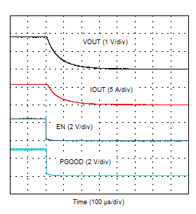
TPS54J061 EN
            Shutdown
VIN = 12 V RLOAD = 0.3 Ω
Figure 7-18 EN Shutdown
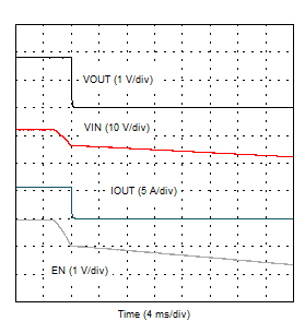
TPS54J061 VIN
            Shutdown
RLOAD = 0.3 Ω
Figure 7-20 VIN Shutdown
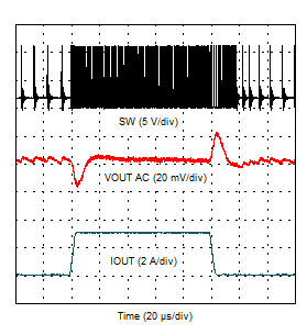
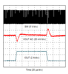
TPS54J061 Load Transient
            – DCM
VIN = 12 V 0.1 A to 3.1 A step 1 A /µsec
MODE = DCM
Figure 7-22 Load Transient – DCM
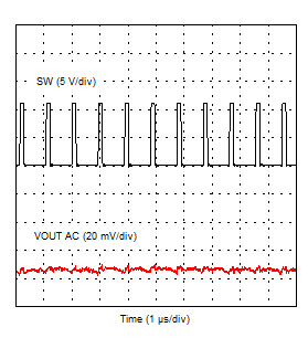
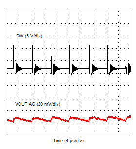
TPS54J061 Output Voltage
            Ripple
VIN = 12 V ILOAD = 0.1 A MODE = FCCM
Figure 7-24 Output Voltage Ripple
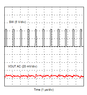
TPS54J061 Output Voltage
            Ripple
VIN = 12 V ILOAD = 6 A
Figure 7-26 Output Voltage Ripple
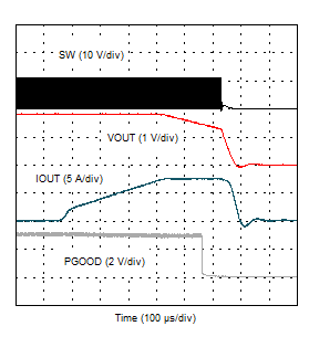
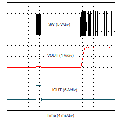
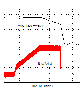
TPS54J061 Overcurrent
            Response
VIN = 12 V IOUT = 7.5-A Constant Current
Figure 7-28 Overcurrent Response
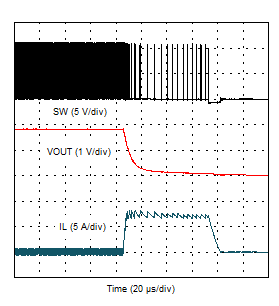
TPS54J061 Short Circuit
            Response
VIN = 12 V IOUT = Short
Figure 7-30 Short Circuit Response
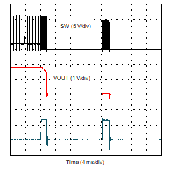
TPS54J061 Overcurrent Exit Hiccup
VIN = 12 V IOUT = 7.5-A Constant Current
Figure 7-32 Overcurrent Exit Hiccup
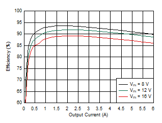
TPS54J061 Efficiency –
            1100 kHz, DCM
VOUT = 1.8 V fSW = 1100 kHz MODE = DCM
VCC = Int 3.0 V
Figure 7-3 Efficiency – 1100 kHz, DCM
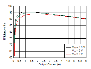
TPS54J061 Efficiency –
            1100 kHz, FCCM, External 3.3-V VCC, 0-Ω RBOOT
VOUT = 1.8 V fSW = 1100 kHz MODE = FCCM
VCC = Ext 3.3 V RBOOT = 0 Ω
Figure 7-5 Efficiency – 1100 kHz, FCCM, External 3.3-V VCC, 0-Ω RBOOT
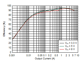
TPS54J061 Efficiency –
            1100 kHz, DCM, External 3.3-V VCC, 0-Ω RBOOT
VOUT = 1.8 V fSW = 1100 kHz MODE = DCM
VCC = Ext 3.3 V RBOOT = 0 Ω
Figure 7-7 Efficiency – 1100 kHz, DCM, External 3.3-V VCC, 0-Ω RBOOT
TPS54J061 Efficiency –
            600 kHz, DCM
VOUT = 1.8 V fSW = 600 kHz MODE = DCM
VCC = Int 3.0 V
Figure 7-9 Efficiency – 600 kHz, DCM
TPS54J061 Output Voltage
            vs Output Current – DCM
VOUT = 1.8 V fSW = 1100 kHz MODE = DCM
Figure 7-11 Output Voltage vs Output Current – DCM
TPS54J061 Switching
            Frequency vs Output Current – 1100 kHz
VOUT = 1.8 V fSW = 1100 kHz MODE = FCCM
Figure 7-13 Switching Frequency vs Output Current – 1100 kHz
TPS54J061 EN
            Start-Up
VIN = 12 V RLOAD = 0.3 Ω
Figure 7-15 EN Start-Up
TPS54J061 EN Start-Up –
            DCM
VIN = 12 V IOUT = 0 A MODE = DCM
Figure 7-17 EN Start-Up – DCM
TPS54J061 VIN
            Start-Up
RLOAD = 0.3 Ω
Figure 7-19 VIN Start-Up
TPS54J061 Load Transient
            – FCCM
VIN = 12 V 0.1 A to 3.1 A step 1 A/µsec
MODE = FCCM
Figure 7-21 Load Transient – FCCM
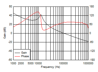
TPS54J061 Bode Plot
VIN = 12 V IOUT = 6 A
Figure 7-23 Bode Plot
TPS54J061 Output Voltage
            Ripple – DCM
VIN = 12 V ILOAD = 0.1 A MODE = DCM
Figure 7-25 Output Voltage Ripple – DCM
TPS54J061 EN Start-Up
            With Prebias
VIN = 12 V IOUT = 0 A Prebias = 1.0 V
Figure 7-27 EN Start-Up With Prebias
TPS54J061 Overcurrent
            Response
VIN = 12 V IOUT = 7.5-A Constant Current
Figure 7-29 Overcurrent Response
TPS54J061 Overcurrent Enter Hiccup
VIN = 12 V IOUT = 7.5-A Constant Current
Figure 7-31 Overcurrent Enter Hiccup