JAJSKM9B July 2020 – November 2020 TPS54JB20
PRODUCTION DATA
- 1 特長
- 2 アプリケーション
- 3 概要
- 4 Revision History
- 5 Pin Configuration and Functions
- 6 Specifications
-
7 Detailed Description
- 7.1 Overview
- 7.2 Functional Block Diagram
- 7.3
Feature Description
- 7.3.1 Internal VCC LDO And Using External Bias On VCC Pin
- 7.3.2 Enable
- 7.3.3 Output Voltage Setting
- 7.3.4 Internal Fixed Soft Start and External Adjustable Soft Start
- 7.3.5 External REFIN For Output Voltage Tracking
- 7.3.6 Frequency and Operation Mode Selection
- 7.3.7 D-CAP3 Control
- 7.3.8 Low-side FET Zero-Crossing
- 7.3.9 Current Sense and Positive Overcurrent Protection
- 7.3.10 Low-side FET Negative Current Limit
- 7.3.11 Power Good
- 7.3.12 Overvoltage and Undervoltage Protection
- 7.3.13 Out-Of-Bounds (OOB) Operation
- 7.3.14 Output Voltage Discharge
- 7.3.15 UVLO Protection
- 7.3.16 Thermal Shutdown
- 7.4 Device Functional Modes
-
8 Application and Implementation
- 8.1 Application Information
- 8.2
Typical Application
- 8.2.1 Design Requirements
- 8.2.2
Detailed Design Procedure
- 8.2.2.1 Output Voltage Setting Point
- 8.2.2.2 Choose the Switching Frequency and the Operation Mode
- 8.2.2.3 Choose the Inductor
- 8.2.2.4 Set the Current Limit (TRIP)
- 8.2.2.5 Choose the Output Capacitor
- 8.2.2.6 Choose the Input Capacitors (CIN)
- 8.2.2.7 Soft Start Capacitor (SS/REFIN Pin)
- 8.2.2.8 EN Pin Resistor Divider
- 8.2.2.9 VCC Bypass Capacitor
- 8.2.2.10 BOOT Capacitor
- 8.2.2.11 Series BOOT Resistor and RC Snubber
- 8.2.2.12 PGOOD Pullup Resistor
- 8.2.3 Application Curves
- 9 Power Supply Recommendations
- 10Layout
- 11Device and Documentation Support
- 12Mechanical, Packaging, and Orderable Information
8.2.2.3 Choose the Inductor
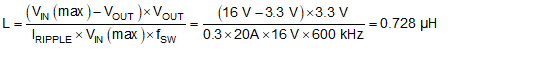
To calculate the value of the output inductor (LOUT), use Equation 9. The output capacitor filters the inductor-ripple current (IIND(ripple)). Therefore, selecting a high inductor-ripple current impacts the selection of the output capacitor because the output capacitor must have a ripple-current rating equal to or greater than the inductor-ripple current. On the other hand, larger ripple current increases output ripple voltage, but improves signal-to-noise ratio and helps to stabilize operation. Generally speaking, the inductance value should set the ripple current at approximately 15% to 40% of the maximum output current for a balanced performance.
For this design, the inductor-ripple current is set to 30% of output current. With a 0.6-MHz switching frequency, 16 V as maximum VIN, and 3.3 V as the output voltage, the calculated inductance is 0.728 μH. A nearest standard value of 0.80 µH is chosen.
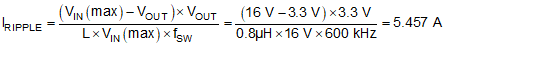
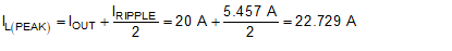
The inductor requires a low DCR to achieve good efficiency. The inductor also requires enough room above peak inductor current before saturation. The peak inductor current is estimated using Equation 10. For this design, by selecting 6.04 A as the RTRIP, IOC(valley) is set to 20 A, thus peak inductor current under maximum VIN is calculated as 5.457 A.
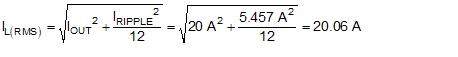
The selected inductance is a Coilcraft XAL7070-801. This has a saturation current rating of 37.8 A , RMS current rating of and a DCR of 2.29 mΩ max. This inductor was selected for its low DCR to get high efficiency.