JAJSNP4A May 2023 – February 2024 TPS54KB20
PRODUCTION DATA
- 1
- 1 特長
- 2 アプリケーション
- 3 概要
- 4 Pin Configuration and Functions
- 5 Specifications
-
6 Detailed Description
- 6.1 Overview
- 6.2 Functional Block Diagram
- 6.3
Feature Description
- 6.3.1 Internal VCC LDO and Using External Bias On the VCC Pin
- 6.3.2 Enable
- 6.3.3 Adjustable Soft Start
- 6.3.4 Power Good
- 6.3.5 Output Voltage Setting
- 6.3.6 Remote Sense
- 6.3.7 D-CAP4 Control
- 6.3.8 Multifunction Select (MSEL) Pin
- 6.3.9 Low-side MOSFET Zero-Crossing
- 6.3.10 Current Sense and Positive Overcurrent Protection
- 6.3.11 Low-side MOSFET Negative Current Limit
- 6.3.12 Overvoltage and Undervoltage Protection
- 6.3.13 Output Voltage Discharge
- 6.3.14 UVLO Protection
- 6.3.15 Thermal Shutdown
- 6.4 Device Functional Modes
-
7 Application and Implementation
- 7.1 Application Information
- 7.2
Typical Application
- 7.2.1 Design Requirements
- 7.2.2
Detailed Design Procedure
- 7.2.2.1 Output Voltage Setting Point
- 7.2.2.2 Choose the Switching Frequency and the Operation Mode
- 7.2.2.3 Choose the Inductor
- 7.2.2.4 Set the Current Limit (ILIM)
- 7.2.2.5 Choose the Output Capacitor
- 7.2.2.6 RAMP Selection
- 7.2.2.7 Choose the Input Capacitors (CIN)
- 7.2.2.8 Soft-Start Capacitor (SS Pin)
- 7.2.2.9 EN Pin Resistor Divider
- 7.2.2.10 VCC Bypass Capacitor
- 7.2.2.11 BOOT Capacitor
- 7.2.2.12 RC Snubber
- 7.2.2.13 PG Pullup Resistor
- 7.2.3 Application Curves
- 7.3 Power Supply Recommendations
- 7.4 Layout
- 8 Device and Documentation Support
- 9 Revision History
- 10Mechanical, Packaging, and Orderable Information
7.2.3 Application Curves

| VOUT = 3.3V | VVCC = 3V internal | fSW = 800kHz |
| LOUT = 470nH | DCR = 1.85mΩ | Skip-mode |
 Figure 7-4 Load Regulation
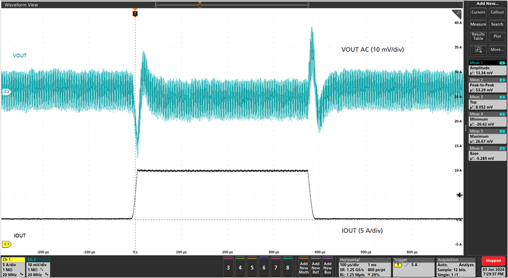
| IOUT = 5A to 15A at 1A/μs | ||
| RMSEL = 86.6kΩ | fSW = 800kHz | RAMP1 |
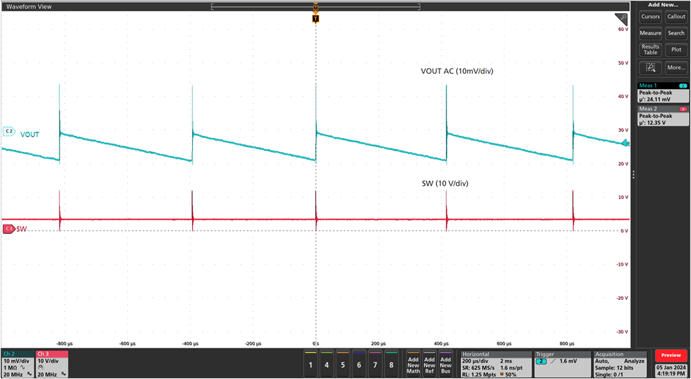
| VIN = 12V | VOUT = 3.3V | IOUT = 10mA |
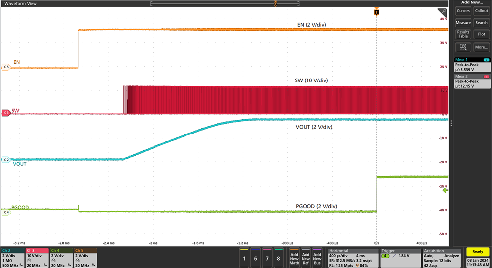
| VIN = 12V | VOUT = 3.3V | IOUT = 25A |

| VOUT = 3.3V | VVCC = 3V internal | fSW = 800kHz |
| LOUT = 470nH | DCR = 1.85mΩ | FCCM |
 Figure 7-5 Line Regulation
| IOUT = 10A | ||
| RMSEL = 86.6kΩ | fSW = 800kHz | RAMP1 |
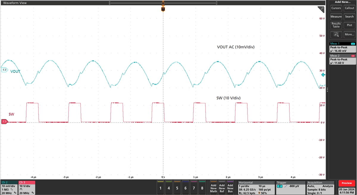
| VIN = 12V | VOUT = 3.3V | IOUT = 25A |
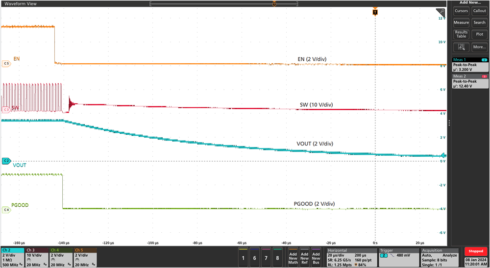
| VIN = 12V | VOUT = 3.3V | IOUT = 25A |