JAJSTW1 August 2024 TPS55287-Q1
PRODUCTION DATA
- 1
- 1 特長
- 2 アプリケーション
- 3 概要
- 4 Pin Configuration and Functions
- 5 Specifications
-
6 Detailed Description
- 6.1 Overview
- 6.2 Functional Block Diagram
- 6.3
Feature Description
- 6.3.1 VCC Power Supply
- 6.3.2 EXTVCC Power Supply
- 6.3.3 I2C Address Selection
- 6.3.4 Input Undervoltage Lockout
- 6.3.5 Enable and Programmable UVLO
- 6.3.6 Soft Start
- 6.3.7 Shutdown and Load Discharge
- 6.3.8 Switching Frequency
- 6.3.9 Switching Frequency Dithering
- 6.3.10 Inductor Current Limit
- 6.3.11 Internal Charge Path
- 6.3.12 Output Voltage Setting
- 6.3.13 Output Current Monitoring and Cable Voltage Droop Compensation
- 6.3.14 Output Current Limit
- 6.3.15 Overvoltage Protection
- 6.3.16 Output Short Circuit Protection
- 6.3.17 Thermal Shutdown
- 6.4 Device Functional Modes
- 6.5 Programming
-
7 Register Maps
- 7.1 REF Register (Address = 0h, 1h) [reset = 10100100b, 00000001b]
- 7.2 IOUT_LIMIT Register (Address = 2h) [reset = 11100100b]
- 7.3 VOUT_SR Register (Address = 3h) [reset = 00000001b]
- 7.4 VOUT_FS Register (Address = 4h) [reset = 00000011b]
- 7.5 CDC Register (Address = 5h) [reset = 11100000b]
- 7.6 MODE Register (Address = 6h) [reset = 00100000b]
- 7.7 STATUS Register (Address = 7h) [reset = 00000011b]
- 7.8 Register Summary
- 8 Application and Implementation
- 9 Device and Documentation Support
- 10Revision History
- 11Mechanical, Packaging, and Orderable Information
パッケージ・オプション
デバイスごとのパッケージ図は、PDF版データシートをご参照ください。
メカニカル・データ(パッケージ|ピン)
- RYQ|21
サーマルパッド・メカニカル・データ
- RYQ|21
発注情報
6.3.5 Enable and Programmable UVLO
The TPS55287-Q1 has a dual function enable and undervoltage lockout (UVLO) circuit. When the input voltage at the VIN pin is above the input UVLO rising threshold of 3V and the EN/UVLO pin is pulled above 1.15V but less than the enable UVLO threshold of 1.23V, the TPS55287-Q1 is enabled but still in standby mode. The TPS55287-Q1 starts to detect the MODE pin logic status and select the I2C target address.
The EN/UVLO pin has an accurate UVLO voltage threshold to support programmable input undervoltage lockout with hysteresis. When the EN/UVLO pin voltage is greater than the UVLO threshold of 1.23V, the TPS55287-Q1 is enabled for I2C communication and switching operation. A hysteresis current IUVLO_HYS is sourced out of the EN/UVLO pin to provide hysteresis that prevents on/off chattering in the presence of noise with a slowly changing input voltage.
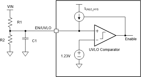
By using resistor divider as shown in Figure 6-1, the turn-on threshold is calculated using Equation 1.

where
- VUVLO is the UVLO threshold of 1.23V at the EN/UVLO pin
The hysteresis between the UVLO turn-on threshold and turn-off threshold is set by the upper resistor in the EN/UVLO resistor divider and is given by the Equation 2.

where
- IUVLO_HYS is the sourcing current from the EN/UVLO pin when the voltage at the EN/UVLO pin is above VUVLO
 Figure 6-1 Programmable UVLO With
Resistor Divider at the EN/UVLO Pin
Figure 6-1 Programmable UVLO With
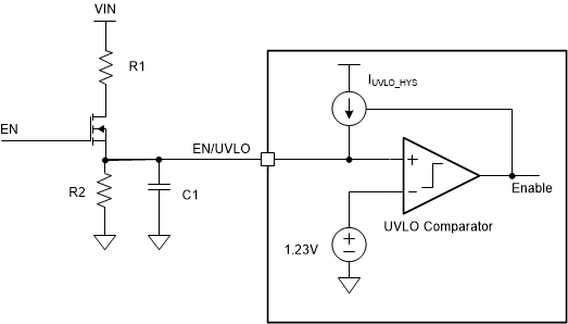
Resistor Divider at the EN/UVLO PinUsing an NMOSFET together with a resistor divider can implement both logic enable and programmable UVLO as shown in Figure 6-2. The EN logic high level must be greater than enable threshold plus the Vth of the NMOSFET Q1. The Q1 also eliminates the leakage current from VIN to ground through the UVLO resistor divider during shutdown mode.
 Figure 6-2 Logic Enable and Programmable
UVLO