JAJSO99 april 2023 TPS552892-Q1
PRODUCTION DATA
- 1
- 1 特長
- 2 アプリケーション
- 3 説明
- 4 Revision History
- 5 Pin Configuration and Functions
- 6 Specifications
-
7 Detailed Description
- 7.1 Overview
- 7.2 Functional Block Diagram
- 7.3
Feature Description
- 7.3.1 VCC Power Supply
- 7.3.2 EXTVCC Power Supply
- 7.3.3 Input Undervoltage Lockout
- 7.3.4 Enable and Programmable UVLO
- 7.3.5 Soft Start
- 7.3.6 Shutdown
- 7.3.7 Switching Frequency
- 7.3.8 Switching Frequency Dithering
- 7.3.9 Inductor Current Limit
- 7.3.10 Internal Charge Path
- 7.3.11 Output Voltage Setting
- 7.3.12 Output Current Monitoring and Cable Voltage Droop Compensation
- 7.3.13 Output Current Limit
- 7.3.14 Overvoltage Protection
- 7.3.15 Output Short Circuit Protection
- 7.3.16 Power Good
- 7.3.17 Constant Current Output Indication
- 7.3.18 Thermal Shutdown
- 7.4 Device Functional Modes
- 8 Application and Implementation
- 9 Device and Documentation Support
- 10Mechanical, Packaging, and Orderable Information
7.3.4 Enable and Programmable UVLO
The TPS552892-Q1 has a dual function enable and undervoltage lockout (UVLO) circuit. When the input voltage at the VIN pin is above the input UVLO rising threshold of 3 V and the EN/UVLO pin is pulled above 1.15 V but less than the enable UVLO threshold of 1.23 V, the TPS552892-Q1 is enabled but still in standby mode. The TPS552892-Q1 starts to detect the MODE pin logic status.
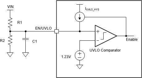
The EN/UVLO pin has an accurate UVLO voltage threshold to support programmable input undervoltage lockout with hysteresis. When the EN/UVLO pin voltage is greater than the UVLO threshold of 1.23 V, the TPS552892-Q1 is enabled for switching operation. A hysteresis current IUVLO_HYS is sourced out of the EN/UVLO pin to provide hysteresis that prevents on/off chattering in the presence of noise with a slowly changing input voltage.
By using resistor divider as shown in Figure 7-1, the turnon threshold is calculated using Equation 1.

where
- VUVLO is the UVLO threshold of 1.23 V at the EN/UVLO pin
The hysteresis between the UVLO turnon threshold and turnoff threshold is set by the upper resistor in the EN/UVLO resistor divider and is given by the Equation 2.

where
- IUVLO_HYS is the sourcing current from the EN/UVLO pin when the voltage at the EN/UVLO pin is above VUVLO
 Figure 7-1 Programmable UVLO With Resistor Divider at the
EN/UVLO Pin
Figure 7-1 Programmable UVLO With Resistor Divider at the
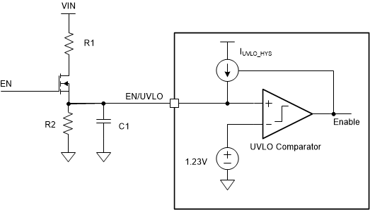
EN/UVLO PinUsing an NMOSFET together with a resistor divider can implement both logic enable and programmable UVLO as shown in Figure 7-2. The EN logic high level must be greater than enable threshold plus the Vth of the NMOSFET Q1. The Q1 also eliminates the leakage current from VIN to ground through the UVLO resistor divider during shutdown mode.
 Figure 7-2 Logic Enable
and Programmable UVLO