SLVS939B June 2009 – December 2014 TPS55332-Q1
PRODUCTION DATA.
- 1 Features
- 2 Applications
- 3 Description
- 4 Revision History
- 5 Pin Configuration and Functions
- 6 Specifications
-
7 Detailed Description
- 7.1 Overview
- 7.2 Functional Block Diagram
- 7.3
Feature Description
- 7.3.1 Input Voltage (VIN)
- 7.3.2 Output Voltage (Vout)
- 7.3.3 Regulated Supply Voltage (VReg)
- 7.3.4 Over-Current Protection (SW)
- 7.3.5 Oscillator Frequency (RT)
- 7.3.6 Enable / Shutdown (EN)
- 7.3.7 Reset Delay (Cdly)
- 7.3.8 Reset Pin (RST)
- 7.3.9 Boost Capacitor (BOOT)
- 7.3.10 Soft Start (SS)
- 7.3.11 Synchronization (SYNC)
- 7.3.12 Regulation Voltage (VSENSE)
- 7.3.13 Reset Threshold (RST_TH)
- 7.3.14 Slew Rate Control (Rslew)
- 7.3.15 Thermal Shutdown
- 7.3.16 Loop Control Frequency Compensation
- 7.4 Device Functional Modes
-
8 Application and Implementation
- 8.1 Application Information
- 8.2
Typical Application
- 8.2.1 Design Requirements
- 8.2.2
Detailed Design Procedure
- 8.2.2.1 Output Capacitor (Co)
- 8.2.2.2 Output Inductor Selection (Lo) for CCM
- 8.2.2.3 Output Diode
- 8.2.2.4 Input Capacitor CI
- 8.2.2.5 Output Voltage And Feedback Resistor Selection
- 8.2.2.6 Reset Threshold Resistor Selection
- 8.2.2.7 Soft Start Capacitor
- 8.2.2.8 Loop Compensation Calculation
- 8.2.2.9 Loop Compensation Response
- 8.2.2.10 Output Inductor Selection (LO) For DCM
- 8.2.3 Application Curves
- 9 Power Supply Recommendations
- 10Layout
- 11Device and Documentation Support
- 12Mechanical, Packaging, and Orderable Information
パッケージ・オプション
メカニカル・データ(パッケージ|ピン)
- PWP|20
サーマルパッド・メカニカル・データ
- PWP|20
発注情報
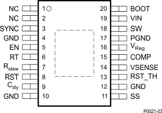
5 Pin Configuration and Functions
PWP Package
20 Pins
(Top View)

Pin Functions
| PIN | I/O | DESCRIPTION | |
|---|---|---|---|
| NAME | NO. | ||
| NC | 1 | NC | Connect to ground |
| NC | 2 | NC | Connect to ground |
| SYNC | 3 | I | External synchronization clock input, 62-kΩ (typ) pull-down resistor |
| GND | 4 | I | Connect to ground |
| EN | 5 | I | Enable input, high voltage tolerant |
| RT | 6 | O | Resistor to program internal oscillator frequency |
| Rslew | 7 | O | Internal switch programmable slew rate control |
| RST | 8 | O | Reset output open drain (active low) |
| Cdly | 9 | O | Reset delay timer (programmed by external capacitor) |
| GND | 10 | O | Analog ground, DVSS and SUB |
| SS | 11 | O | Programmable soft-start. (external capacitor) |
| GND | 12 | I | Connect to ground |
| RST_TH | 13 | I | Input for RESET circuitry to detect undervoltage on output (adjustable threshold) |
| VSENSE | 14 | I | Feedback input for voltage mode control |
| COMP | 15 | O | Error amplifier output |
| VReg | 16 | I | Internal low side FET to load output during start up or limit over shoot |
| PGND | 17 | O | Power ground connection |
| SW | 18 | I/O | Switched drain output/input |
| VIN | 19 | I | Unregulated input voltage |
| BOOT | 20 | O | Bootstrap capacitor pump |