JAJSJK1D December   2015  – September 2024 TPS562201 , TPS562208

PRODUCTION DATA  

  1.   1
  2. 特長
  3. アプリケーション
  4. 概要
  5. Pin Configuration and Functions
  6. Specifications
    1. 5.1 Absolute Maximum Ratings
    2. 5.2 ESD Ratings
    3. 5.3 Recommended Operating Conditions
    4. 5.4 Thermal Information
    5. 5.5 Electrical Characteristics
    6. 5.6 Typical Characteristics
  7. Detailed Description
    1. 6.1 Overview
    2. 6.2 Functional Block Diagram
    3. 6.3 Feature Description
      1. 6.3.1 Adaptive On-Time Control and PWM Operation
      2. 6.3.2 Pulse Skip Control (TPS562201)
      3. 6.3.3 Soft Start and Prebiased Soft Start
      4. 6.3.4 Current Protection
      5. 6.3.5 Undervoltage Lockout (UVLO) Protection
      6. 6.3.6 Thermal Shutdown
    4. 6.4 Device Functional Modes
      1. 6.4.1 Normal Operation
      2. 6.4.2 Eco-mode Operation
      3. 6.4.3 Standby Operation
  8. Application and Implementation
    1. 7.1 Application Information
    2. 7.2 Typical Application
      1. 7.2.1 Design Requirements
      2. 7.2.2 Detailed Design Procedure
        1. 7.2.2.1 Custom Design with WEBENCH® Tools
        2. 7.2.2.2 Output Voltage Resistors Selection
        3. 7.2.2.3 Output Filter Selection
        4. 7.2.2.4 Input Capacitor Selection
        5. 7.2.2.5 Bootstrap Capacitor Selection
      3. 7.2.3 Application Curves
    3. 7.3 Power Supply Recommendations
    4. 7.4 Layout
      1. 7.4.1 Layout Guidelines
      2. 7.4.2 Layout Example
  9. Device and Documentation Support
    1. 8.1 Device Support
      1. 8.1.1 Development Support
        1. 8.1.1.1 Custom Design with WEBENCH® Tools
    2. 8.2 ドキュメントの更新通知を受け取る方法
    3. 8.3 サポート・リソース
    4. 8.4 Trademarks
    5. 8.5 静電気放電に関する注意事項
    6. 8.6 用語集
  10. Revision History
  11. 10Mechanical, Packaging, and Orderable Information
    1. 10.1 Tape and Reel Information

パッケージ・オプション

メカニカル・データ(パッケージ|ピン)
サーマルパッド・メカニカル・データ
発注情報

Pin Configuration and Functions

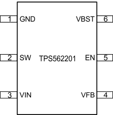
TPS562201 TPS562208 6-Pin SOT DDC Package (Top
                    View) Figure 4-1 6-Pin SOT DDC Package (Top View)
Table 4-1 Pin Functions
PIN DESCRIPTION
NAME NO.
GND 1 Ground pin source terminal of low-side power NFET as well as the ground terminal for controller circuit. Connect sensitive VFB to this GND at a single point.
SW 2 Switch node connection between high-side NFET and low-side NFET
VIN 3 Input voltage supply pin. The drain terminal of high-side power NFET
VFB 4 Converter feedback input. Connect to output voltage with feedback resistor divider.
EN 5 Enable input control. Active high and must be pulled up to enable the device
VBST 6 Supply input for the high-side NFET gate drive circuit. Connect a 0.1-µF capacitor between VBST and SW pins.