JAJSL53
October 2021
TPS563212
PRODUCTION DATA
1
特長
2
アプリケーション
3
概要
4
Revision History
5
Pin Configuration and Functions
6
Specifications
6.1
Absolute Maximum Ratings
6.2
ESD Ratings
6.3
Recommended Operating Conditions
6.4
Thermal Information
6.5
Electrical Characteristics
6.6
Typical Characteristics
7
Detailed Description
7.1
Overview
7.2
Functional Block Diagram
7.3
Feature Description
7.3.1
Advanced Emulated Current Mode Control
7.3.2
Mode Selection and PG/SS Pin Function Configuration
7.3.3
Power Good (PG)
7.3.4
Soft Start and Pre-Biased Soft Start
7.3.5
Output Discharge Through PG/SS Pin
7.3.6
Precise Enable and Adjusting Undervoltage Lockout
7.3.7
Overcurrent Limit and Undervoltage Protection
7.3.8
Overvoltage Protection
7.3.9
Thermal Shutdown
7.4
Device Functional Modes
7.4.1
Shutdown Mode
7.4.2
Active Mode
7.4.3
FCCM Operation
7.4.4
CCM Operation
7.4.5
DCM Operation and Eco-mode Operation
7.4.6
On-Time Extension for Large Duty Cycle Operation
8
Application and Implementation
8.1
Application Information
8.2
Typical Application
8.2.1
Design Requirements
8.2.2
Detailed Design Procedure
8.2.2.1
Custom Design With WEBENCH® Tools
8.2.2.2
Output Voltage Resistors Selection
8.2.2.3
Output Inductor Selection
8.2.2.4
Output Capacitor Selection
8.2.2.5
Input Capacitor Selection
8.2.2.6
Bootstrap Capacitor Selection
8.2.2.7
Undervoltage Lockout Set Point
8.2.3
Application Curves
9
Power Supply Recommendations
10
Layout
10.1
Layout Guidelines
10.2
Layout Example
11
Device and Documentation Support
11.1
Device Support
11.1.1
Third-Party Products Disclaimer
11.1.2
Development Support
11.1.2.1
Custom Design With WEBENCH® Tools
11.2
Receiving Notification of Documentation Updates
11.3
サポート・リソース
11.4
Trademarks
11.5
Electrostatic Discharge Caution
11.6
Glossary
12
Mechanical, Packaging, and Orderable Information
パッケージ・オプション
メカニカル・データ(パッケージ|ピン)
DRL|8
MPCS002E
サーマルパッド・メカニカル・データ
発注情報
jajsl53_oa
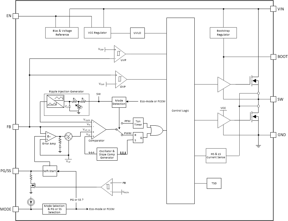
7.2
Functional Block Diagram