JAJSDG1B March 2016 – December 2017 TPS564208
PRODUCTION DATA.
- 1 特長
- 2 アプリケーション
- 3 概要
- 4 改訂履歴
- 5 Pin Configuration and Functions
- 6 Specifications
- 7 Detailed Description
- 8 Application and Implementation
- 9 Power Supply Recommendations
- 10Layout
- 11デバイスおよびドキュメントのサポート
- 12メカニカル、パッケージ、および注文情報
10 Layout
10.1 Layout Guidelines
- VIN and GND traces should be as wide as possible to reduce trace impedance. The wide areas are also of advantage from the view point of heat dissipation.
- The input capacitor and output capacitor should be placed as close to the device as possible to minimize trace impedance.
- Provide sufficient vias for the input capacitor and output capacitor.
- Keep the SW trace as physically short and wide as practical to minimize radiated emissions.
- Do not allow switching current to flow under the device.
- A separate VOUT path should be connected to the upper feedback resistor.
- Make a Kelvin connection to the GND pin for the feedback path.
- Voltage feedback loop should be placed away from the high-voltage switching trace, and preferably has ground shield.
- The trace of the VFB node should be as small as possible to avoid noise coupling.
- The GND trace between the output capacitor and the GND pin should be as wide as possible to minimize its trace impedance.
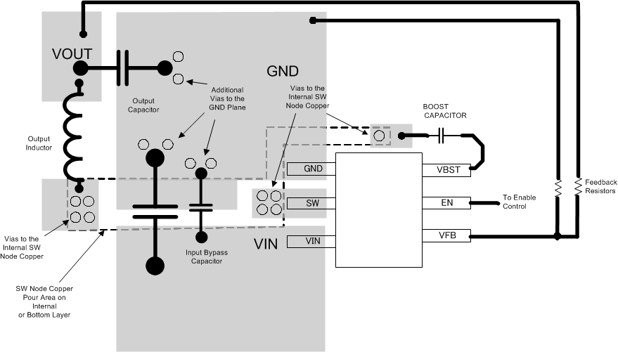
10.2 Layout Example
 Figure 30. TPS564208 Layout Example