JAJSI75A April 2018 – November 2019 TPS57112C-Q1
PRODUCTION DATA.
- 1 特長
- 2 アプリケーション
- 3 概要
- 4 改訂履歴
- 5 概要(続き)
- 6 Pin Configuration and Functions
- 7 Specifications
-
8 Detailed Description
- 8.1 Overview
- 8.2 Functional Block Diagram
- 8.3 Feature Description
- 8.4
Device Functional Modes
- 8.4.1 Adjusting the Output Voltage
- 8.4.2 Enable Functionality and Adjusting Undervoltage Lockout
- 8.4.3 Slow-Start or Tracking Pin
- 8.4.4 Sequencing
- 8.4.5 Constant Switching Frequency and Timing Resistor (RT/CLK Pin)
- 8.4.6 Overcurrent Protection
- 8.4.7 Frequency Shift
- 8.4.8 Reverse Overcurrent Protection
- 8.4.9 Synchronize Using the RT/CLK Pin
- 8.4.10 Power Good (PWRGD Pin)
- 8.4.11 Overvoltage Transient Protection
- 8.4.12 Thermal Shutdown
- 8.4.13 Small-Signal Model for Loop Response
- 8.4.14 Simple Small-Signal Model for Peak-Current-Mode Control
- 8.4.15 Small-Signal Model for Frequency Compensation
-
9 Application and Implementation
- 9.1 Application Information
- 9.2
Typical Application
- 9.2.1 Design Requirements
- 9.2.2
Detailed Design Procedure
- 9.2.2.1 Selecting the Switching Frequency
- 9.2.2.2 Output Inductor Selection
- 9.2.2.3 Output Capacitor
- 9.2.2.4 Input Capacitor
- 9.2.2.5 Slow-Start Capacitor
- 9.2.2.6 Bootstrap Capacitor Selection
- 9.2.2.7 Output Voltage and Feedback Resistor Selection
- 9.2.2.8 Compensation
- 9.2.2.9 Power-Dissipation Estimate
- 9.2.3 Application Curves
- 10Power Supply Recommendations
- 11Layout
- 12デバイスおよびドキュメントのサポート
- 13メカニカル、パッケージ、および注文情報
パッケージ・オプション
メカニカル・データ(パッケージ|ピン)
- RTE|16
サーマルパッド・メカニカル・データ
- RTE|16
発注情報
8.4.14 Simple Small-Signal Model for Peak-Current-Mode Control
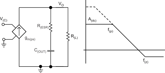
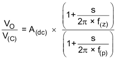
Figure 31 is a simple small-signal model that one can use to understand how to design the frequency compensation. A voltage-controlled current source (duty-cycle modulator) supplying current to the output capacitor and load resistor approximates the TPS57112C-Q1 power stage. Equation 10 shows the control-to-output transfer function, which consists of a dc gain, one dominant pole, and one ESR zero. The quotient of the change in switch current and the change in COMP pin voltage (node c in Figure 31) is the power-stage transconductance. The gm for the TPS57112C-Q1 device is 14 S. The low-frequency gain of the power-stage frequency response is the product of the transconductance and the load resistance, as shown in Equation 11. As the load current increases and decreases, the low-frequency gain decreases and increases, respectively. This variation with load may seem problematic at first glance, but the dominant pole moves with load current [see Equation 12]. The dashed line in the right half of Figure 32 highlights the combined effect. As the load current decreases, the gain increases and the pole frequency lowers, keeping the 0-dB crossover frequency the same for the varying load conditions, which makes it easier to design the frequency compensation.
 Figure 32. Simple Small-Signal Model and Frequency Response for Peak-Current-Mode Control


