JAJSIN7 February 2020 TPS59632-Q1
PRODUCTION DATA.
- 1 特長
- 2 アプリケーション
- 3 概要
- 4 改訂履歴
- 5 Pin Configuration and Functions
- 6 Specifications
-
7 Detailed Description
- 7.1 Overview
- 7.2 Functional Block Diagram
- 7.3
Feature Description
- 7.3.1 PWM Operation
- 7.3.2 Current Sensing
- 7.3.3 Load-line (Droop)
- 7.3.4 Load Transients
- 7.3.5 Overshoot Reduction (OSR)
- 7.3.6 Undershoot Reduction (USR)
- 7.3.7 Autobalance Current Sharing
- 7.3.8 PWM And SKIP Signals
- 7.3.9 Bias Power (V5A, VDD, And VINTF) UVLO
- 7.3.10 Start-Up Sequence
- 7.3.11 Power Good Operation
- 7.3.12 Analog Current Monitor, IMON, And Corresponding Digital Output Current
- 7.3.13 Fault Behavior
- 7.3.14 Output Under Voltage Protection (UVP)
- 7.3.15 Output Over Voltage Protection (OVP)
- 7.3.16 Over Current Protection (OCP)
- 7.3.17 Over Current Warning
- 7.3.18 Input Voltage Limits
- 7.3.19 VID Table
- 7.4 User Selections
- 7.5 I2C Interface Operation
- 7.6 I2C Register Maps
-
8 Applications and Implementation
- 8.1 Application Information
- 8.2
Typical Application
- 8.2.1
3-Phase D-CAP+™, Step-Down Application
- 8.2.1.1 Design Requirements
- 8.2.1.2
Detailed Design Procedure
- 8.2.1.2.1 Step 1: Select Switching Frequency
- 8.2.1.2.2 Step 2: Set The Slew Rate
- 8.2.1.2.3 Step 3: Set The I2C Address
- 8.2.1.2.4 Step 4: Determine Inductor Value And Choose Inductor
- 8.2.1.2.5 Step 5: Current Sensing Resistance
- 8.2.1.2.6 Step 6: Select Over Current Protection (OCP) Setting
- 8.2.1.2.7 Step 7: Current Monitor (IMON) Setting
- 8.2.1.2.8 Step 8: Set the Load-Line Slope
- 8.2.1.2.9 Step 9: Voltage Feedback Resistor Calculation
- 8.2.1.2.10 Step 10: Ramp Compensation Selection
- 8.2.1.2.11 Step 11 Overshoot Reduction (OSR) selection
- 8.2.1.2.12 Step 12: Undershoot Reduction (USR) selection
- 8.2.1.2.13 Step 13: Loop Compensation
- 8.2.1.3 Application Performance Plots
- 8.2.1
3-Phase D-CAP+™, Step-Down Application
- 9 Power Supply Recommendations
- 10Layout
- 11デバイスおよびドキュメントのサポート
- 12メカニカル、パッケージ、および注文情報
7.3.3 Load-line (Droop)
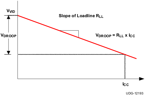
The TPS59632-Q1 features programmable droop enabling significant reduction of output capacitors. Figure 10 shows the output voltage droop with increasing load current.
 Figure 10. Load-Line Slope
 Equation 1. 

where
- RCS(eff) is the effective current sense resistance, when using either a sense resistor or inductor DCR
- ACS is the gain of the current sense amplifier
- ICC is the load current
- ADROOP is the DROOP gain (see Equation 2)
Equation 2. 

where
- resistor, RDROOP is connected between the DROOP pin and the COMP pin
- resistor RCOMP is connected between the COMP pin and the VREF pin
This load-line aids in the transient performance as discussed in the following section.