SLVS888C December 2008 – October 2015 TPS60150
PRODUCTION DATA.
6 Specifications
6.1 Absolute Maximum Ratings
Over operating free-air temperature range (unless otherwise noted) (1)| MIN | MAX | UNIT | ||
|---|---|---|---|---|
| VIN | Input voltage (all pins) | –0.3 | 7 | V |
| TA | Operating temperature | –40 | 85 | °C |
| TJ | Maximum operating junction temperature | 150 | °C | |
| Tstg | Storage temperature | –55 | 150 | °C |
(1) Stresses beyond those listed under Absolute Maximum Ratings may cause permanent damage to the device. These are stress ratings only and functional operation of the device at these or any other conditions beyond those indicated under recommended operating conditions is not implied. Exposure to absolute-maximum-rated conditions for extended periods may affect device reliability.
6.2 ESD Ratings
| VALUE | UNIT | |||
|---|---|---|---|---|
| V(ESD) | Electrostatic discharge | Human body model (HBM), per ANSI/ESDA/JEDEC JS-001(1)(2) | ±2000 | V |
| Charged-device model (CDM), per JEDEC specification JESD22-C101(3) | ±500 | |||
(1) JEDEC document JEP155 states that 500-V HBM allows safe manufacturing with a standard ESD control process.
(2) The human body model (HBM) is a 100-pF capacitor discharged through a 1.5-kΩ resistor into each pin. The testing is done according JEDECs EIA/JESD22-A114.
(3) JEDEC document JEP157 states that 250-V CDM allows safe manufacturing with a standard ESD control process.
6.3 Recommended Operating Conditions
6.4 Thermal Information
| THERMAL METRIC(1) | TPS60150 | UNIT | |
|---|---|---|---|
| DRV (WSON) | |||
| 6 PINS | |||
| RθJA | Junction-to-ambient thermal resistance | 69.1 | °C/W |
| RθJC(top) | Junction-to-case (top) thermal resistance | 79.8 | °C/W |
| RθJB | Junction-to-board thermal resistance | 38.6 | °C/W |
| ψJT | Junction-to-top characterization parameter | 1.2 | °C/W |
| ψJB | Junction-to-board characterization parameter | 38.4 | °C/W |
| RθJC(bot) | Junction-to-case (bottom) thermal resistance | 9.2 | °C/W |
(1) For more information about traditional and new thermal metrics, see the IC Package Thermal Metrics application report, SPRA953.
6.5 Electrical Characteristics
VIN = 3.6 V, TA = –40°C to 85°C, typical values are at TA = 25°C, C1 = C3 = 2.2 μF, C2 = 1 μF (unless otherwise noted)| PARAMETER | TEST CONDITIONS | MIN | TYP | MAX | UNIT | |
|---|---|---|---|---|---|---|
| POWER STAGE | ||||||
| VIN | Input voltage range | 2.7 | 5.5 | V | ||
| VUVLO | Undervoltage lockout threshold | 1.9 | 2.1 | V | ||
| IQ | Operating quiescent current | IOUT = 140 mA, Enable = VIN | 4.7 | mA | ||
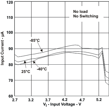
| IQskip | Skip mode operating quiescent current | IOUT = 0 mA, Enable=VIN (no switching) | 80 | μA | ||
| IOUT = 0 mA, Enable = VIN(minimum switching) | 90 | μA | ||||
| ISD | Shut down current | 2.7 V ≤ VIN ≤ 5.5 V, Enable = 0 V | 1 | μA | ||
| VOUT | Output voltage(1) | IOUT ≤ 50 mA, 2.7 V ≤ VIN < 5.5 V | 4.8 | 5 | 5.2 | V |
| VOUT(skip) | Skip mode output voltage | IOUT = 0 mA, 2.7 V ≤ VIN ≤ 5.5 V | VOUT + 0.1 | V | ||
| FSW | Switching frequency | 1.5 | MHz | |||
| SSTIME | Soft-start time | From the rising edge of enable to 90% output | 150 | μs | ||
| OUTPUT CURRENT | ||||||
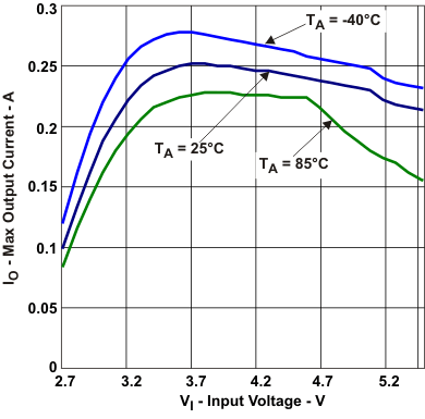
| IOUT_nom | Maximum output current | VOUT remains from 4.8 V to 5.2 V, 3.1 V ≤ VIN ≤ 5.5 V |
120 | mA | ||
| 3.3 V < VIN < 5.5 V | 140 | |||||
| IOUT_short | Short circuit current(2) | VOUT = 0 V | 80 | mA | ||
| RIPPLE VOLTAGE | ||||||
| VR | Output ripple voltage | IOUT = 140 mA | 30 | mV | ||
| ENABLE CONTROL | ||||||
| VHI | Logic high input voltage | 2.7 V ≤ VIN ≤ 5.5 V | 1.3 | VIN | V | |
| VLI | Logic low input voltage | –0.2 | 0.4 | V | ||
| IHI | Logic high input current | 1 | μA | |||
| ILI | Logic low input current | 1 | μA | |||
| THERMAL SHUTDOWN | ||||||
| TSD | Shutdown temperature | 160 | °C | |||
| TRC | Shutdown recovery | 140 | °C | |||
(1) When in skip mode, output voltage can exceed VOUT spec because VOUT(skip) = VOUT+0.1.
(2) The TPS60150 device has internal protection circuit to protect IC when VOUT shorted to GND.
6.6 Typical Characteristics

