SLVS372C June 2001 – October 2015 TPS60240 , TPS60241 , TPS60242 , TPS60243
PRODUCTION DATA.
- 1 Features
- 2 Applications
- 3 Description
- 4 Revision History
- 5 Pin Configuration and Functions
- 6 Specifications
- 7 Detailed Description
- 8 Application and Implementation
- 9 Power Supply Recommendations
- 10Layout
- 11Device and Documentation Support
- 12Mechanical, Packaging, and Orderable Information
パッケージ・オプション
デバイスごとのパッケージ図は、PDF版データシートをご参照ください。
メカニカル・データ(パッケージ|ピン)
- DGK|8
サーマルパッド・メカニカル・データ
発注情報
1 Features
- Wide Input Voltage Range from 1.8 V to 5.5 V
- Regulated 2.7-V, 3-V, 3.3-V or 5-V Output Voltage With ±2.5% Accuracy Over Load
- Up to 25-mA Output Current
- 170-µVrms Zero Ripple Output:
at 20 Hz to 10 MHz Bandwidth - Up to 90% Efficiency
- Minimum Number of External Components
- No Inductors
- Only Small Ceramic Chip Capacitors
- Shutdown Mode: 0.1 µA Typical
- Thermal Protection and Current Limit
- Micro-Small 8-Pin VSSOP Package
- EVM Available TPS60241EVM-194
2 Applications
- VCO and PLL Power for:
- Smart Phones
- Mobile Phones
- PCMCIA Modems
- Smartcard Readers
- Digital Cameras
- MP3 Players
- SIM Modules
- Electronic Games
- Memory Backup
- Handheld Meters
- Bias Supplies
3 Description
The TPS6024x devices are a family of switched capacitor voltage converters, ideally suited for voltage-controlled oscillator (VCO) and phase-locked loop (PLL) applications that require low noise and tight tolerances. Its dual-cap design uses four ceramic capacitors to provide ultra-low output ripple with high efficiency, while eliminating the need for inefficient linear regulators.
The TPS6024x devices operate down to 1.8 V, supporting a 3.3-V, 2.7-V, 3-V output from two-cell, nickel- or alkaline-based chemistries, whereas the TPS60241 works with 2.7-V to 5.5-V input voltage providing a 5-V output. The devices work equally well for low EMI DC–DC step-up conversion without the need for an inductor. The high switching frequency (typical 160 kHz) promotes the use of small surface-mount capacitors, saving board space. The shutdown mode of the converter conserves battery energy.
The devices are thermally protected and current-limited for reliable operation even under persisting fault conditions. Normal quiescent current (ground pin current) is only 250 µA, and typically 0.1 µA in shutdown mode. The TPS6024x devices come in a thin, 8-pin VSSOP package with a component height of only 1.1 mm.
Device Information(1)
| PART NUMBER | PACKAGE | OUTPUT VOLTAGE |
|---|---|---|
| TPS60240 | VSSOP (8) | 3.3 V |
| TPS60241 | 5 V | |
| TPS60242 | 2.7 V | |
| TPS60243 | 3 V |
- For all available packages, see the orderable addendum at the end of the data sheet.
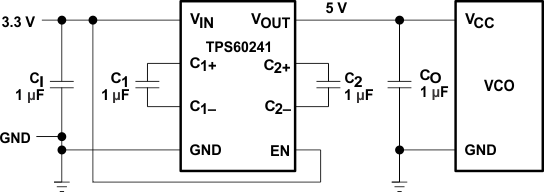
Typical Application Schematic

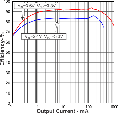
Efficiency vs Output Current
