SLVS302B December 2000 – October 2015 TPS60300 , TPS60301 , TPS60302 , TPS60303
PRODUCTION DATA.
- 1 Features
- 2 Applications
- 3 Description
- 4 Revision History
- 5 Description (continued)
- 6 Device Comparison Table
- 7 Pin Configuration and Functions
- 8 Specifications
- 9 Detailed Description
- 10Application and Implementation
- 11Power Supply Recommendations
- 12Layout
- 13Device and Documentation Support
- 14Mechanical, Packaging, and Orderable Information
12 Layout
12.1 Layout Guidelines
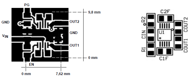
All capacitors must be soldered as close as possible to the IC. A PCB layout proposal for a two-layer board is shown in Figure 24. Care has been taken to connect all capacitors as close as possible to the circuit to achieve optimized output voltage ripple performance. The bottom layer is not shown in Figure 24. It only consists of a ground-plane with a single track between the two vias that can be seen in the left part of the top layer.
12.2 Layout Example
 Figure 24. Recommended PCB Layout for TPS6030x (Top Layer)
12.3 Power Dissipation
The thermal resistance of the unsoldered package is RθJA = 294°C/W. Soldered on the EVM, a typical thermal resistance of RθJA(EVM) = 200°C/W was measured.
The thermal resistance can be calculated as shown in Equation 4.

where
- TJ is the junction temperature.
- TA is the ambient temperature.
- PD is the power that needs to be dissipated by the device.
The maximum power dissipation can be calculated as shown in Equation 5.
The maximum power dissipation happens with maximum input voltage and maximum output current:
At maximum load the supply current is approximately 2 mA.
With this maximum rating and the thermal resistance of the device on the EVM, the maximum temperature rise above ambient temperature can be calculated as shown in Equation 7.
This means that internal dissipation increases TJ by 10°C.
The junction temperature of the device must not exceed 125°C.
This means the IC can easily be used at ambient temperatures as seen in Equation 8.