SGLS246B June 2004 – October 2016 TPS60400-Q1 , TPS60401-Q1 , TPS60402-Q1 , TPS60403-Q1
PRODUCTION DATA.
- 1 Features
- 2 Applications
- 3 Description
- 4 Revision History
- 5 Device Comparison Table
- 6 Pin Configuration and Functions
- 7 Specifications
- 8 Detailed Description
- 9 Application and Implementation
- 10Power Supply Recommendations
- 11Layout
- 12Device and Documentation Support
- 13Mechanical, Packaging, and Orderable Information
パッケージ・オプション
デバイスごとのパッケージ図は、PDF版データシートをご参照ください。
メカニカル・データ(パッケージ|ピン)
- DBV|5
サーマルパッド・メカニカル・データ
発注情報
7 Specifications
7.1 Absolute Maximum Ratings
over operating free-air temperature range (unless otherwise noted)(1)| MIN | MAX | UNIT | ||
|---|---|---|---|---|
| Voltage range | IN to GND | –0.3 | 5.5 | V |
| OUT to GND | –5 | 0.3 | ||
| CFLY– to GND | 0.3 | VO – 0.3 | ||
| CFLY+ to GND | –0.3 | VI + 0.3 | ||
| Continuous power dissipation | See Thermal Information | |||
| Continuous output current | 80 | mA | ||
| Maximum junction temperature, TJ | 150 | °C | ||
| Storage temperature, Tstg | –55 | 150 | °C | |
(1) Stresses beyond those listed under Absolute Maximum Ratings may cause permanent damage to the device. These are stress ratings only, which do not imply functional operation of the device at these or any other conditions beyond those indicated under Recommended Operating Conditions. Exposure to absolute-maximum-rated conditions for extended periods may affect device reliability.
7.2 ESD Ratings
| VALUE | UNIT | |||
|---|---|---|---|---|
| V(ESD) | Electrostatic discharge | Human-body model (HBM), per AEC Q100-002(1) | ±2000 | V |
| Charged-device model (CDM), per AEC Q100-011 | ±1000 | |||
(1) AEC Q100-002 indicates that HBM stressing shall be in accordance with the ANSI/ESDA/JEDEC JS-001 specification.
7.3 Recommended Operating Conditions
over operating free-air temperature range (unless otherwise noted)| MIN | NOM | MAX | UNIT | ||
|---|---|---|---|---|---|
| VI | Input voltage | 1.8 | 5.25 | V | |
| IO | Output current at OUT | 60 | mA | ||
| CI | Input capacitor | 0 | C(fly)(1) | µF | |
| C(fly) | Flying capacitor | 1 | µF | ||
| CO | Output capacitor | 1 | 100 | µF | |
| TJ | Operating junction temperature | –40 | 125 | °C | |
(1) Refer to Device Comparison Table for Cfly values
7.4 Thermal Information
| THERMAL METRIC(1) | TPS6040x-Q1 | UNIT | |
|---|---|---|---|
| DBV (SOT-25) | |||
| 5 PINS | |||
| RθJA | Junction-to-ambient thermal resistance | 221.2 | °C/W |
| RθJC(top) | Junction-to-case (top) thermal resistance | 81.9 | °C/W |
| RθJB | Junction-to-board thermal resistance | 39.8 | °C/W |
| ψJT | Junction-to-top characterization parameter | 3.3 | °C/W |
| ψJB | Junction-to-board characterization parameter | 38.9 | °C/W |
| RθJC(bot) | Junction-to-case (bottom) thermal resistance | N/A | °C/W |
(1) For more information about traditional and new thermal metrics, see the Semiconductor and IC Package Thermal Metrics.
7.5 Electrical Characteristics
CI = C(fly) = CO (according to Table 2), TJ = –40°C to 125°C, and VI = 5 V over recommended operating free-air temperature range (unless otherwise noted)| PARAMETER | TEST CONDITIONS | MIN | TYP | MAX | UNIT | ||
|---|---|---|---|---|---|---|---|
| VI | Supply voltage range | At TJ = –40°C to 125°C, RL = 5 kΩ | 1.8 | 5.25 | V | ||
| At TC ≥ 0°C, RL = 5 kΩ | 1.6 | ||||||
| IO | Maximum output current at VO | 60 | mA | ||||
| VO | Output voltage | –VI | V | ||||
| VP–P | Output voltage ripple | IO = 5 mA | TPS60400-Q1, C(fly) = 1 µF, CO = 2.2 µF |
35 | mVP–P | ||
| TPS60401-Q1, C(fly) = CO = 10 µF |
20 | ||||||
| TPS60402-Q1, C(fly) = CO = 3.3 µF |
20 | ||||||
| TPS60403-Q1, C(fly) = CO = 1 µF |
15 | ||||||
| IQ | Quiescent current (no-load input current) |
VI = 5 V | TPS60400-Q1 | 125 | 270 | µA | |
| TPS60401-Q1 | 65 | 190 | |||||
| TPS60402-Q1 | 120 | 270 | |||||
| TPS60403-Q1 | 425 | 700 | |||||
| TJ = 60°C, VI = 5 V |
TPS60400-Q1 | 210 | |||||
| TPS60401-Q1 | 135 | ||||||
| TPS60402-Q1 | 210 | ||||||
| TPS60403-Q1 | 640 | ||||||
| fOSC | Internal switching frequency | TPS60400-Q1, VCO version | 25 | 50 to 250 | 375 | kHz | |
| TPS60401-Q1 | 10 | 20 | 30 | ||||
| TPS60402-Q1 | 25 | 50 | 75 | ||||
| TPS60403-Q1 | 115 | 250 | 325 | ||||
| Impedance at 25°C, VI = 5 V | TPS60400-Q1, CI = C(fly) = CO = 1 µF | 12 | 15 | Ω | |||
| TPS60401-Q1, CI = C(fly) = CO = 10 µF | 12 | 15 | |||||
| TPS60402-Q1, CI = C(fly) = CO = 3.3 µF | 12 | 15 | |||||
| TPS60403-Q1, CI = C(fly) = CO = 1 µF | 12 | 15 | |||||
7.6 Typical Characteristics
Table 1. Table of Graphs
| FIGURE | |||
|---|---|---|---|
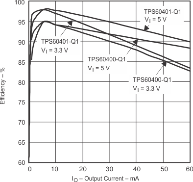
| η | Efficiency | vs Output current at 3.3 V and 5 V (TPS6040x-Q1) | Figure 1, Figure 2 |
| II | Input current | vs Output current (TPS6040x-Q1) | Figure 3, Figure 4 |
| IS | Supply current | vs Input voltage (TPS6040x-Q1) | Figure 5, Figure 6 |
| Output resistance | vs Input voltage at –40°C, 0°C, 25°C, 85°C CI = C(fly) = CO = 1 µF (TPS60400-Q1) CI = C(fly) = CO = 10 µF (TPS60401-Q1) CI = C(fly) = CO = 3.3 µF (TPS60402-Q1) CI = C(fly) = CO = 1 µF (TPS60403-Q1) |
Figure 7, Figure 8, Figure 9, Figure 10 | |
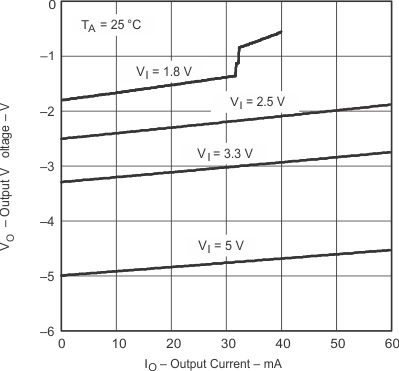
| VO | Output voltage | vs Output current at 25°C, VIN = 1.8 V, 2.5 V, 3.3 V, 5 V CI = C(fly) = CO = 1 µF (TPS60400-Q1) CI = C(fly) = CO = 10 µF (TPS60401-Q1) CI = C(fly) = CO = 3.3 µF (TPS60402-Q1) CI = C(fly) = CO = 1 µF (TPS60403-Q1) |
Figure 11, Figure 12, Figure 13, Figure 14 |
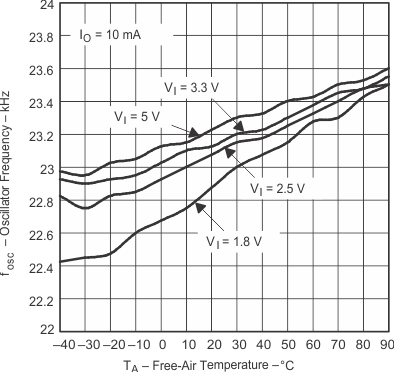
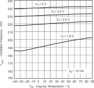
| fOSC | Oscillator frequency | vs Temperature at VI = 1.8 V, 2.5 V, 3.3 V, 5 V (TPS6040x-Q1) | Figure 15, Figure 16, Figure 17, Figure 18 |
| vs Output current TPS60400 at 2 V, 3.3 V, 5 V | Figure 19 | ||
| Output ripple and noise | VI = 5 V, IO = 30 mA, CI = C(fly) = CO = 1 µF (TPS60400-Q1) VI = 5 V, IO = 30 mA, CI = C(fly) = CO = 10 µF (TPS60401-Q1) VI = 5 V, IO = 30 mA, CI = C(fly) = CO = 3.3 µF (TPS60402-Q1) VI = 5 V, IO = 30 mA, CI = C(fly) = CO = 1 µF (TPS60403-Q1) |
Figure 24, Figure 25 | |
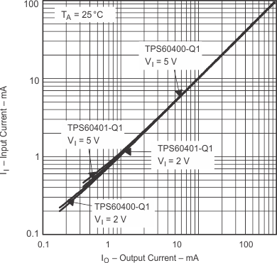
Input Current vs Output Current
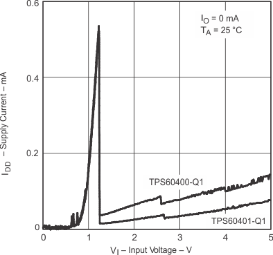
Supply Current vs Input Voltage
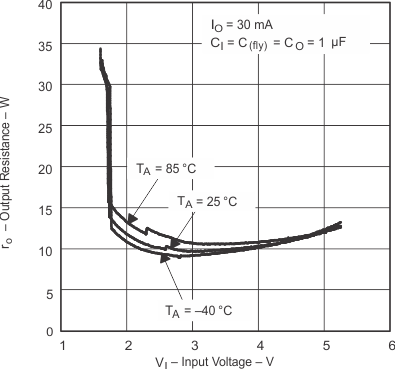
vs Input Voltage
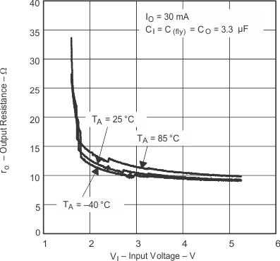
vs Input Voltage
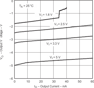
vs Output Current
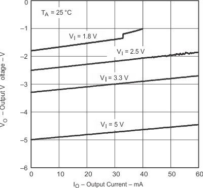
vs Output Current
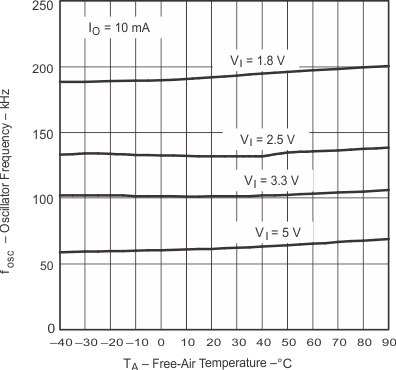
vs Free-Air Temperature
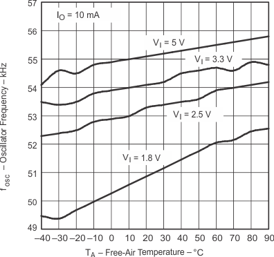
vs Free-Air Temperature
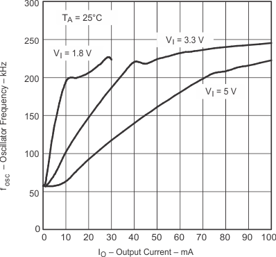
vs Output Current
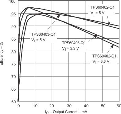
Efficiency vs Output Current
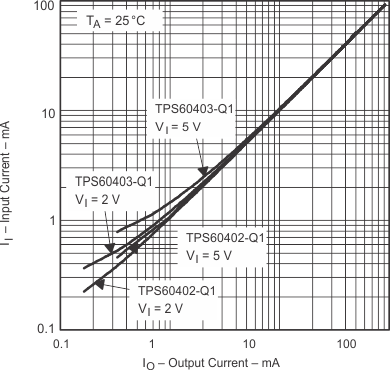
Input Current vs Output Current
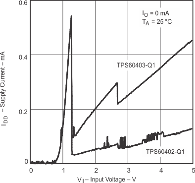
Supply Current vs Input Voltage
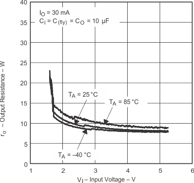
vs Input Voltage
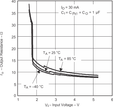
vs Input Voltage
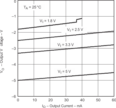
vs Output Current
vs Output Current
vs Free-Air Temperature
vs Free-Air Temperature
