SLVSCF2A January 2014 – December 2014 TPS61097A-33
PRODUCTION DATA.
- 1 Features
- 2 Applications
- 3 Description
- 4 Revision History
- 5 Pin Configuration and Functions
- 6 Specifications
- 7 Parameter Measurement Information
- 8 Detailed Description
- 9 Application and Implementation
- 10Power Supply Recommendations
- 11Layout
- 12Device and Documentation Support
- 13Mechanical, Packaging, and Orderable Information
1 Features
- Up to 93% Efficiency at Typical Operating Conditions
- Connection from Battery to Load via Bypass Switch in Shutdown Mode
- Typical Shutdown Current Less Than 5 nA
- Typical Quiescent Current Less Than 5 μA
- Operating Input Voltage Range
From 0.9 V to 5.5 V - Power-Save Mode for Improved Efficiency at Low Output Power
- Overtemperature Protection
- Small 2.8-mm x 2.9-mm 5-Pin SOT-23 Package
2 Applications
- MSP430 Applications
- All Single-Cell, Two-Cell, and Three-Cell Alkaline, NiCd, NiMH, or Single-Cell Li-Battery Powered Products
- Personal Medical Products
- Fuel Cell and Solar Cell Powered Products
- PDAs
- Mobile Applications
- White LEDs
3 Description
The TPS61097A-33 provides a power supply solution for products powered by either a single-cell, two-cell, or three-cell alkaline, NiCd, or NiMH, or one-cell Li-Ion or Li-polymer battery. They can also be used in fuel cell or solar cell powered devices where the capability of handling low input voltages is essential. Possible output currents depend on the input-to-output voltage ratio. The devices provide output currents up to 100 mA at a 3.3-V output while using a single-cell Li-Ion or Li-Polymer battery. The boost converter is based on a current-mode controller using synchronous rectification to obtain maximum efficiency. The maximum average input current is limited to a value of 400 mA. The converter can be disabled to minimize battery drain. During shutdown, the battery is connected to the load to enable battery backup of critical functions on the load. The device is packaged in a 5-pin SOT-23 package (DBV) measuring 2.8 mm × 2.9 mm.
Device Information(1)
| PART NUMBER | PACKAGE | BODY SIZE (NOM) |
|---|---|---|
| TPS61097A-33 | SOT-23 (5) | 2.90 mm × 2.90 mm |
- For all available packages, see the orderable addendum at the end of the datasheet.
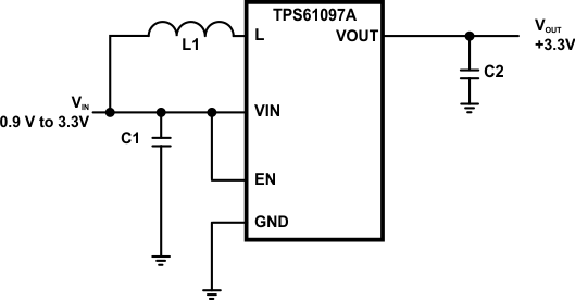
Typical Operating Application