JAJSL22F June   2015  – September 2021 TPS61098 , TPS610981 , TPS610982 , TPS610985 , TPS610986 , TPS610987

PRODUCTION DATA  

  1. 特長
  2. アプリケーション
  3. 概要
  4. Revision History
  5. Device Comparison Table
  6. Pin Configuration and Functions
  7. Specifications
    1. 7.1 Absolute Maximum Ratings
    2. 7.2 ESD Ratings
    3. 7.3 Recommended Operating Conditions
    4. 7.4 Thermal Information
    5. 7.5 Electrical Characteristics
    6. 7.6 Typical Characteristics
  8. Detailed Description
    1. 8.1 Overview
    2. 8.2 Functional Block Diagrams
    3. 8.3 Feature Description
      1. 8.3.1 Boost Controller Operation
      2. 8.3.2 Pass-Through Operation
      3. 8.3.3 LDO / Load Switch Operation
      4. 8.3.4 Start Up and Power Down
      5. 8.3.5 Over Load Protection
      6. 8.3.6 Thermal Shutdown
    4. 8.4 Device Functional Modes
      1. 8.4.1 Operation Modes by MODE Pin
        1. 8.4.1.1 Active Mode
        2. 8.4.1.2 Low Power Mode
      2. 8.4.2 Burst Mode Operation under Light Load Condition
      3. 8.4.3 Pass-Through Mode Operation
  9. Applications and Implementation
    1. 9.1 Application Information
    2. 9.2 Typical Applications
      1. 9.2.1 VMAIN to Power MCU and VSUB to Power Subsystem
        1. 9.2.1.1 Design Requirements
        2. 9.2.1.2 Detailed Design Procedure
          1. 9.2.1.2.1 Device Choice
          2. 9.2.1.2.2 Maximum Output Current
          3. 9.2.1.2.3 Inductor Selection
          4. 9.2.1.2.4 Capacitor Selection
          5. 9.2.1.2.5 Control Sequence
        3. 9.2.1.3 Application Curves
      2. 9.2.2 VMAIN to Power the System in Low Power Mode
        1. 9.2.2.1 Design Requirements
        2. 9.2.2.2 Detailed Design Procedure
        3. 9.2.2.3 Application Curves
      3. 9.2.3 VSUB to Power the System in Active Mode
        1. 9.2.3.1 Design Requirements
        2. 9.2.3.2 Detailed Design Procedure
        3. 9.2.3.3 Application Curves
  10. 10Power Supply Recommendations
  11. 11Layout
    1. 11.1 Layout Guidelines
    2. 11.2 Layout Example
  12. 12Device and Documentation Support
    1. 12.1 Device Support
      1. 12.1.1 Third-Party Products Disclaimer
    2. 12.2 Documentation Support
      1. 12.2.1 Related Documentation
    3. 12.3 Receiving Notification of Documentation Updates
    4. 12.4 サポート・リソース
    5. 12.5 Trademarks
    6. 12.6 静電気放電に関する注意事項
    7. 12.7 用語集
  13. 13Mechanical, Packaging, and Orderable Information

パッケージ・オプション

メカニカル・データ(パッケージ|ピン)
サーマルパッド・メカニカル・データ
発注情報

Low Power Mode

The TPS61098x works in Low Power mode when MODE pin is logic low. In Low Power mode, the LDO/load switch is turned off, so the peripherals can be disconnected to minimize the battery drain. The VSUB pin either outputs high impedance or is pulled to ground by internal active discharge circuit, depending on different versions. The boost converter consumes only 300 nA quiescent current typically, and can achieve up to 88% efficiency at 10 µA load.

The Low Power mode is designed to keep the load device powered with minimum power consumption. For example, it can be used to keep powering the main system, like an MCU, in a system's sleep mode even under < 0.7 V input voltage condition.

Figure 8-3 and Figure 8-4 illustrate the outputs of the TPS61098 and TPS610981 under different input voltages in Active mode and Low Power mode.
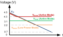
GUID-81420E51-B71A-4EB7-BDAB-F9DCA9A9FEA2-low.gifFigure 8-3 TPS61098 Output under Different Input Voltages
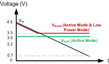
GUID-1A1175E3-565D-44D1-B5E1-85B833158E63-low.gifFigure 8-4 TPS610981 Output under Different Input Voltages

The TPS610982 is an exception. Its LDO is always on in both Active mode and Low Power mode with higher quiescent current consumption than other versions. The TPS610982 can be used to replace discrete boost and LDO solutions where the LDO output is always on, and its two modes provide users two options of different quiescent current consumption and performance. Refer to Section 8.4.1, Section 7 and Section 7.6 for details.