SLVSBM5B December 2012 – August 2015 TPS61176
PRODUCTION DATA.
- 1 Features
- 2 Applications
- 3 Description
- 4 Revision History
- 5 Pin Configuration and Functions
- 6 Specifications
- 7 Detailed Description
- 8 Application and Implementation
- 9 Power Supply Recommendations
- 10Layout
- 11Device and Documentation Support
- 12Mechanical, Packaging, and Orderable Information
パッケージ・オプション
メカニカル・データ(パッケージ|ピン)
- RTE|16
サーマルパッド・メカニカル・データ
- RTE|16
発注情報
6 Specifications
6.1 Absolute Maximum Ratings
over operating free-air temperature range (unless otherwise noted)(1)| MIN | MAX | UNIT | ||
|---|---|---|---|---|
| Voltage range(2) | VIN, PWM/EN, MODE/FAULT | –0.3 | 7 | V |
| SW | –0.3 | 40 | V | |
| IFB1 to IFB6 | –0.3 | 20 | V | |
| All other pins | –0.3 | 3.6 | V | |
| Continuous power dissipation | See Thermal Information | |||
| Operating junction temperature | –40 | 150 | °C | |
| Storage temperature, Tstg | –65 | 150 | °C | |
(1) Stresses beyond those listed under Absolute Maximum Ratings may cause permanent damage to the device. These are stress ratings only, which do not imply functional operation of the device at these or any other conditions beyond those indicated under Recommended Operating Conditions. Exposure to absolute-maximum-rated conditions for extended periods may affect device reliability.
(2) All voltage values are with respect to network ground terminal.
6.2 ESD Ratings
| VALUE | UNIT | |||
|---|---|---|---|---|
| V(ESD) | Electrostatic discharge | Human-body model (HBM), per ANSI/ESDA/JEDEC JS-001(1) | ±4000 | V |
| Charged-device model (CDM), per JEDEC specification JESD22-C101(2) | ±2000 | |||
| Machine model | ±200 | |||
(1) JEDEC document JEP155 states that 500-V HBM allows safe manufacturing with a standard ESD control process.
(2) JEDEC document JEP157 states that 250-V CDM allows safe manufacturing with a standard ESD control process.
6.3 Recommended Operating Conditions
over operating free-air temperature range (unless otherwise noted)| MIN | NOM | MAX | UNIT | ||
|---|---|---|---|---|---|
| VIN | Bias voltage to device (see Figure 18) | 2.7 | 6.5 | V | |
| Input voltage to inductor (see Figure 18) | 2.7 | 24 | V | ||
| VOUT | Output voltage range | VIN | 38 | V | |
| L | Inductor | 4.7 | 6.8 | 10 | µH |
| CI | Input capacitor | 1.0 | 2.2 | µF | |
| CO | Output capacitor | 2.2 | 4.7 | 10 | µF |
| CCOMP | COMP capacitor | 0.47 | 1 | µF | |
| FPWM_I | Input PWM signal frequency | 0.1 | 22 | kHz | |
| TA | Operating ambient temperature | –40 | 85 | °C | |
| TJ | Operating junction temperature | –40 | 125 | °C | |
6.4 Thermal Information
| THERMAL METRIC(1) | TPS61176 | UNIT | |
|---|---|---|---|
| RTE (WQFN) | |||
| 16 PINS | |||
| RθJA | Junction-to-ambient thermal resistance | 43 | °C/W |
| RθJC(top) | Junction-to-case (top) thermal resistance | 44.4 | °C/W |
| RθJB | Junction-to-board thermal resistance | 14.4 | °C/W |
| ψJT | Junction-to-top characterization parameter | 0.6 | °C/W |
| ψJB | Junction-to-board characterization parameter | 14.3 | °C/W |
| RθJC(bot) | Junction-to-case (bottom) thermal resistance | 3.3 | °C/W |
(1) For more information about traditional and new thermal metrics, see the Semiconductor and IC Package Thermal Metrics application report, SPRA953.
6.5 Electrical Characteristics
VIN = 3.6 V, PWM/EN = high, IFB current = 20 mA, IFB voltage = 450 mV, TA = –40°C to +85°C, typical values are at TA = 25°C (unless otherwise noted).| PARAMETER | TEST CONDITIONS | MIN | TYP | MAX | UNIT | |
|---|---|---|---|---|---|---|
| POWER SUPPLY | ||||||
| VIN | Input voltage range | 2.7 | 6.5 | V | ||
| VIN_UVLO | VIN undervoltage lockout threshold | VIN ramp down | 2.4 | 2.5 | V | |
| VIN ramp up | 2.65 | 2.7 | ||||
| VIN_HYS | VIN undervoltage lockout hysteresis | 250 | mV | |||
| Iq_VIN | Operating quiescent current into VIN | Device enable, switching 1 MHz and no load | 3 | mA | ||
| ISD | Shutdown current | PWM/EN = low | 1 | 4 | µA | |
| PWM/EN = low, TA = 25°C | 1 | 2 | ||||
| VLDO | VLDO pin output voltage | VIN = 3.6 V | 3 | 3.3 | 3.5 | V |
| PWM/EN | ||||||
| VH | PWM/EN logic high | 1.2 | V | |||
| VL | PWM/EN logic Low | 0.4 | V | |||
| RPD | PWM/EN pin internal pull-down resistor | 400 | 800 | 1600 | kΩ | |
| tSD | PWM/EN logic low width to shutdown | PWM/EN from high to low | 20 | ms | ||
| CURRENT REGULATION | ||||||
| VISET | ISET pin voltage | PWM/EN logic high | 1.02 | 1.04 | 1.06 | V |
| KISET | Current multiplier | IISET = 20 μA | 1024 | |||
| IFBx | Current accuracy | IISET = 20 μA, 0°C to 70°C | –2% | 2% | ||
| IISET = 20 µA, –40°C to 85°C | –2.3% | 2.3% | ||||
| Km | (IMAX – IMIN) / (2 x IAVG) | IISET = 20 μA | 0.65% | |||
| IIFBx_leak | IFBx pin leakage current | VIFBx = 10 V, each pin | 1.5 | 5 | µA | |
| VIFBx = 5 V, each pin | 0.5 | 2 | ||||
| IIFBx_max | Current sink max output current | IISET = 35 μA, each pin | 35 | mA | ||
| TFBx_MINON | Current sink minimum on time | IISET = 20 μA, each pin | 0.5 | µs | ||
| fdim | PWM dimming frequency | Mode 1 / Mode 3, 0°C to 70°C | 20 | 22 | 27 | kHz |
| BOOST OUTPUT REGULATION | ||||||
| VIFBx_min | IFBx regulation voltage | Measured on VIFB(MIN), IISET = 20 μA | 450 | mV | ||
| POWER SWITCH | ||||||
| RDS(on) | Switch MOSFET on-resistance | VIN = 3.6 V | 0.25 | 0.4 | Ω | |
| ILEAK_SW | Switch MOSFET leakage current | VSW = 40 V | 2 | µA | ||
| OSCILLATOR | ||||||
| fSW | Oscillator frequency | 0.8 | 1 | 1.2 | MHz | |
| Dmax | Maximum boost switch duty cycle | 93% | ||||
| MODE/FAULT | ||||||
| VMODE | MODE/FAULT pin voltage during mode detection period | Tested as VIN – VMODE when mode resistor is connected between VIN pin and MODE/FAULT pin; Tested as VMODE when mode resistor is connected between MODE/FAULT pin and GND | 0.6 | 0.9 | V | |
| IMODE_PD | MODE/FAULT pin pulldown current after mode detection | VMODE = 0.5 V, mode resistor is connected between VIN pin and MODE/FAULT pin | 50 | 80 | µA | |
| OC, SC, OVP and SS | ||||||
| ILIM | Switch MOSFET current limit | 2 | 2.5 | 3 | A | |
| VOVP_clamp | Output overvoltage clamp threshold | 1.47 | 1.5 | 1.53 | V | |
| VOVP_sd | Output overvoltage shutdown threshold | OVP ramp up | 1.568 | 1.6 | 1.632 | V |
| OVP ramp down | 1.519 | 1.55 | 1.581 | |||
| VOVP_SC | Output short to GND detection threshold | OVP ramp up | 90 | mV | ||
| OVP ramp down | 50 | 70 | ||||
| VOVP_IFB | 1st level IFB overvoltage threshold | IFBx current sink on | 7 | 8.5 | 10 | V |
| VOVP2_IFB | 2nd level IFB overvoltage threshold | IFBx current sink on or off | 16 | 18 | 20 | V |
| THERMAL SHUTDOWN | ||||||
| Tshutdown | Thermal shutdown threshold | 160 | °C | |||
| Thys | Thermal shutdown hysteresis | 15 | °C | |||
6.6 Typical Characteristics
Table 1. Table Of Graphs
| TITLE | DESCRIPTION | FIGURE |
|---|---|---|
| Dimming Efficiency | VBAT = 3 V, 3.6 V, 4.2 V, 5 V; VO = 18 V, 6s6p, 20 mA/string; PWM Freq = 200 Hz; Mode 1; L = 6.8 µH |
Figure 1 |
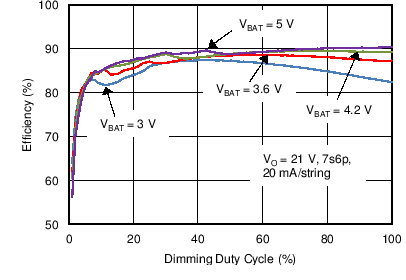
| Dimming Efficiency | VBAT = 3 V, 3.6 V, 4.2 V, 5 V; VO = 21 V, 7s6p, 20 mA/string; PWM Freq = 200 Hz; Mode 1; L = 6.8µH |
Figure 2 |
| Dimming Efficiency | VBAT = 3 V, 3.6 V, 4.2 V, 5 V; VO = 24 V, 8s5p, 20 mA/string; PWM Freq = 200 Hz; Mode 1; L = 6.8 µH |
Figure 3 |
| Dimming Efficiency | VBAT = 3 V, 3.6 V, 4.2 V, 5 V; VO = 27 V, 9s4p, 20 mA/string; PWM Freq = 20 0Hz; Mode 1; L = 6.8µH |
Figure 4 |
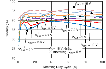
| Dimming Efficiency | VIN = 5 V; VBAT = 3 V, 3.6 V, 4.2 V, 5 V, 7.2 V, 9 V, 12 V, 15 V; VO = 18 V, 6s6p, 20 mA/string; PWM Freq = 200 Hz; Mode 1; L = 6.8 µH (refer to Figure 18) |
Figure 5 |
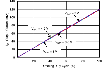
| Dimming Linearity | VBAT = 3 V, 3.6 V, 4.2 V, 5 V; VO = 21 V, 7s6p; RISET = 53 kΩ ; PWM Freq = 200 Hz; Mode 1 |
Figure 6 |
| Current Limit vs Input Voltage | VO = 30 V; TA = 25°C | Figure 7 |
| Switching Waveform | VBAT = 3.6 V; VO = 18 V, 6s6p; RISET = 53 kΩ; Duty = 100%; L = 6.8 µH | Figure 11 |
| Switching Waveform | VBAT = 3.6 V; VO = 18 V, 6s6p; RISET = 53 kΩ; PWM Freq = 200 Hz; Duty = 50%; L = 6.8 µH; Mode 1 |
Figure 12 |
| Switching Waveform | VBAT = 3.6 V; VO = 18 V, 6s6p; RISET = 53 kΩ; PWM Freq = 200 Hz; Duty = 10%; L = 6.8 µH; Mode 1 |
Figure 13 |
| Switching Waveform | VBAT = 3.6 V; VO = 18 V, 6s6p; RISET = 53 kΩ; PWM Freq = 200 Hz; Duty = 50%; L = 6.8 µH; Mode 2 |
Figure 14 |
| Switching Waveform | VBAT = 3.6 V; VO = 18 V, 6s6p; RISET = 53 kΩ; PWM Freq = 200Hz; Duty = 10%; L = 6.8 µH; Mode 2 |
Figure 15 |
| Start-up Waveform | VBAT = 3.6 V; VO = 18 V, 6s6p; RISET = 53 kΩ; Duty = 100%; L = 6.8 µH | Figure 16 |
| Start-up Waveform | VBAT = 3.6 V; VO = 18 V, 6s6p; RISET = 53 kΩ; PWM Freq = 200 Hz; Duty = 10%; L = 6.8 µH; Mode 1 |
Figure 17 |


