SLVSCK4A September 2015 – May 2016 TPS61235P , TPS61236P
PRODUCTION DATA.
- 1 Features
- 2 Applications
- 3 Description
- 4 Revision History
- 5 Device Comparison Table
- 6 Pin Configuration and Functions
- 7 Specifications
-
8 Detailed Description
- 8.1 Overview
- 8.2 Functional Block Diagram
- 8.3
Feature Description
- 8.3.1 Boost Controller Operation
- 8.3.2 Soft Start
- 8.3.3 Enable and Disable
- 8.3.4 Constant Output Voltage and Constant Output Current Operations
- 8.3.5 Over Current Protection
- 8.3.6 Load Status Indication
- 8.3.7 Under voltage Lockout
- 8.3.8 Over Voltage Protection and Reverse Current Block
- 8.3.9 Short Circuit Protection
- 8.3.10 Thermal Shutdown
- 8.4 Device Functional Modes
-
9 Applications and Implementation
- 9.1 Application Information
- 9.2
Typical Applications
- 9.2.1
TPS61236P 3-V to 4.35-V Input, 5-V Output Voltage, 3-A Maximum Output Current
- 9.2.1.1 Design Requirements
- 9.2.1.2 Detailed Design Procedure
- 9.2.1.3 TPS61236P 5-V Output Application Curves
- 9.2.2 TPS61236P 2.3-V to 5-V Input, 5-V 2-A Output Converter
- 9.2.1
TPS61236P 3-V to 4.35-V Input, 5-V Output Voltage, 3-A Maximum Output Current
- 10Power Supply Recommendations
- 11Layout
- 12Device and Documentation Support
- 13Mechanical, Packaging, and Orderable Information
1 Features
- Up to 97% Efficiency Synchronous Boost
- Up to 3.5-A IOUT for 3.3-V to 5-V Conversion
- 10-A 14-mΩ/14-mΩ Internal Power Switches
- Programmable Constant Output Current
- Output Current Monitor
- 10-µA IQ under Light Load Condition
- Boost Status Indication
- True disconnection during shutdown
- Fixed 5.1-V Output Voltage (TPS61235P) or Adjustable Output Voltage from 2.9-V to-5.5 V (TPS61236P)
- 1-MHz Switching Frequency
- Softstart, Current Limit, Over Voltage and Over Thermal Protections
- 2.5 mm x 2.5 mm VQFN Package
2 Applications
- Power Banks, Battery Backup Units
- USB Charging Port
- USB Type-C
- Battery Powered USB Hub
- Tablet PCs
- Battery Powered Products
3 Description
The TPS6123x is a high current, high efficiency synchronous boost converter with constant output current feature for single cell Li-Ion and Li-polymer battery powered products, in a wide range of power bank, tablet, and other portable devices. The IC integrates 14-mΩ/14-mΩ power switches and is capable of delivering up to a 3.5-A output current for 3.3-V to 5-V conversion with up to 97% high efficiency. The device supports a programmable constant output current to control power delivery, so to save power path components and lower total system thermal dissipation effectively.
The device only consumes a 10-µA quiescent current under a light load condition, and can report load status to the system, which make it very suitable for Always-On applications. With the TPS6123x, a simple and flexible system design can be achieved, eliminating external power path components, saving PCB space, and reducing BOM cost.
In shutdown, the output is completely disconnected from the input, and current consumption is reduced to less than 1 µA. Other features like soft start control, reverse current blocking, over voltage protection, and thermal shutdown protection are built-in for system safety.
The devices are available in a 2.5-mm x 2.5-mm VQFN package.
Device Information(1)
| PART NUMBER | PACKAGE | BODY SIZE (NOM) |
|---|---|---|
| TPS61235P | VQFN (9) | 2.50 mm x 2.50 mm |
| TPS61236P | VQFN (9) | 2.50 mm x 2.50 mm |
- For all available packages, see the orderable addendum at the end of the data sheet.
SPACING
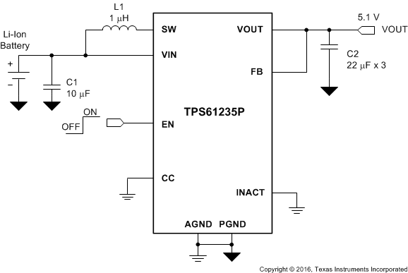
TPS61235P Typical Application

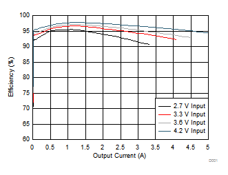
Typical Application Efficiency (TPS61235P)
