SLVSAG8G September   2011  – June 2016 TPS61253 , TPS61254 , TPS61256 , TPS61258 , TPS61259 , TPS612592

UNLESS OTHERWISE NOTED, this document contains PRODUCTION DATA.  

  1. Features
  2. Applications
  3. Description
  4. Revision History
  5. Device Options
  6. Pin Configuration and Functions
  7. Specifications
    1. 7.1 Absolute Maximum Ratings
    2. 7.2 ESD Ratings
    3. 7.3 Recommended Operating Conditions
    4. 7.4 Thermal Information
    5. 7.5 Electrical Characteristics
    6. 7.6 Typical Characteristics
  8. Parameter Measurement Information
  9. Detailed Description
    1. 9.1 Overview
    2. 9.2 Functional Block Diagram
    3. 9.3 Feature Description
      1. 9.3.1 Current Limit Operation
      2. 9.3.2 Enable
      3. 9.3.3 Load Disconnect and Reverse Current Protection
      4. 9.3.4 Softstart
      5. 9.3.5 Undervoltage Lockout
      6. 9.3.6 Thermal Regulation
      7. 9.3.7 Thermal Shutdown
    4. 9.4 Device Functional Modes
      1. 9.4.1 Power Save Mode
      2. 9.4.2 Standby Mode
  10. 10Application and Implementation
    1. 10.1 Application Information
    2. 10.2 Typical Application
      1. 10.2.1 Design Requirements
      2. 10.2.2 Detailed Design Procedure
        1. 10.2.2.1 Inductor Selection
        2. 10.2.2.2 Output Capacitor
        3. 10.2.2.3 Input Capacitor
        4. 10.2.2.4 Checking Loop Stability
      3. 10.2.3 Application Curves
    3. 10.3 System Examples
  11. 11Power Supply Recommendations
  12. 12Layout
    1. 12.1 Layout Guidelines
    2. 12.2 Layout Example
    3. 12.3 Thermal Considerations
  13. 13Device and Documentation Support
    1. 13.1 Device Support
      1. 13.1.1 Third-Party Products Disclaimer
    2. 13.2 Related Links
    3. 13.3 Receiving Notification of Documentation Updates
    4. 13.4 Community Resources
    5. 13.5 Trademarks
    6. 13.6 Electrostatic Discharge Caution
    7. 13.7 Glossary
  14. 14Mechanical, Packaging, and Orderable Information
    1. 14.1 Package Summary
      1. 14.1.1 Package Dimensions

パッケージ・オプション

デバイスごとのパッケージ図は、PDF版データシートをご参照ください。

メカニカル・データ(パッケージ|ピン)
  • YFF|9
サーマルパッド・メカニカル・データ
発注情報

14 Mechanical, Packaging, and Orderable Information

The following pages include mechanical, packaging, and orderable information. This information is the most current data available for the designated devices. This data is subject to change without notice and revision of this document. For browser-based versions of this data sheet, refer to the left-hand navigation.

14.1 Package Summary

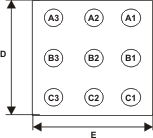
Chip Scale Package
(Bottom View)
TPS61253 TPS61254 TPS61256 TPS61258 TPS61259 TPS612592 po_bott_lvs808.gif

Chip Scale Package
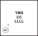
(Top View)

TPS61253 TPS61254 TPS61256 TPS61258 TPS61259 TPS612592 po_top_lvsag8.gif
Code:
  • YM - 2 digit date code
  • S - assembly site code
  • CC - chip code (see ordering table)
  • LLLL - lot trace code

14.1.1 Package Dimensions

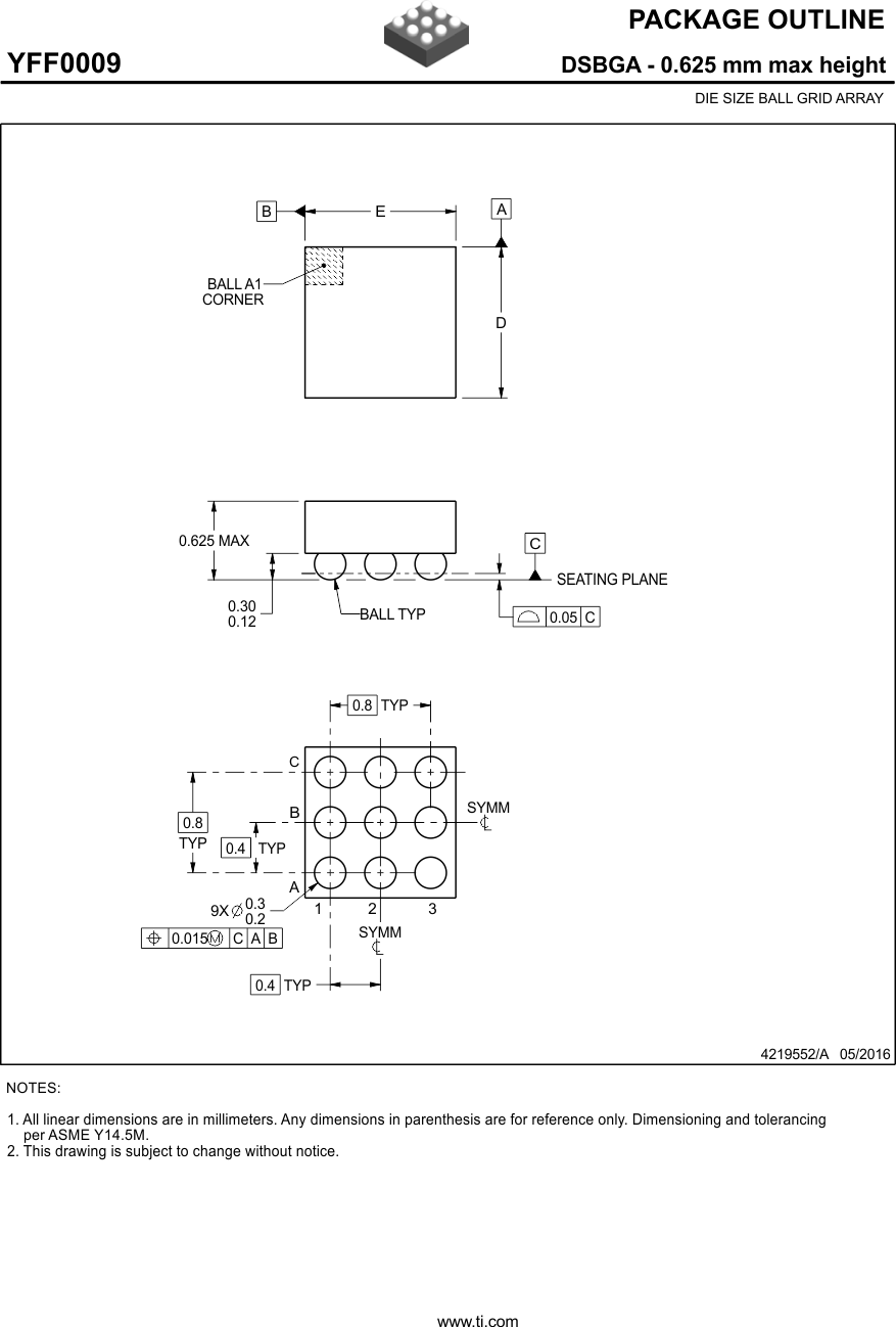
The dimensions for the YFF-9 package are shown in Table 6. See the package drawing at the end of this data sheet.

Table 6. YFF-9 Package Dimensions

PACKAGED DEVICES D E
TPS6125xYFF max = 1.236mm; min = 1.176 mm max = 1.336 mm, min = 1.276 mm
TPS61253 TPS61254 TPS61256 TPS61258 TPS61259 TPS612592 YFF0009_4219552_Page_01.gif
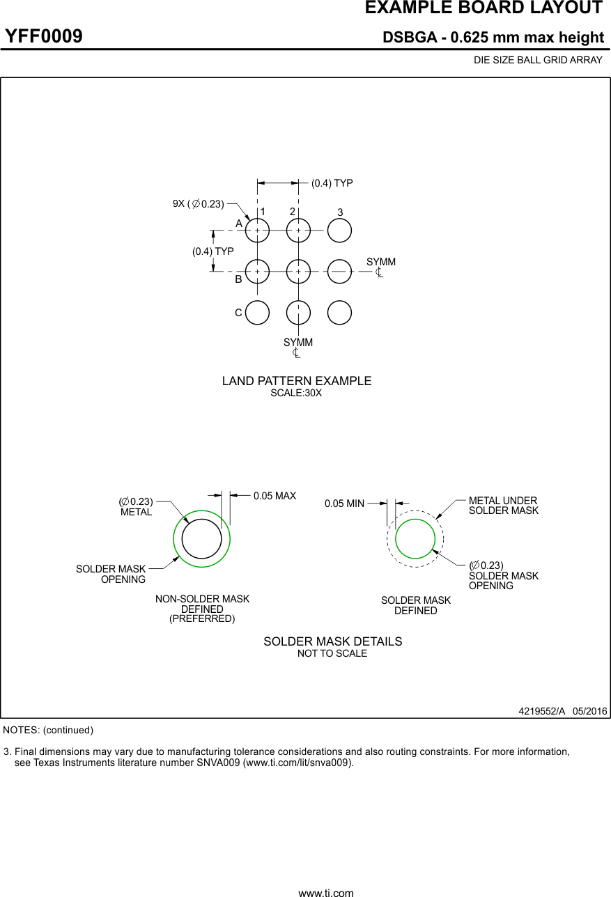
TPS61253 TPS61254 TPS61256 TPS61258 TPS61259 TPS612592 YFF0009_4219552_Page_02.gif
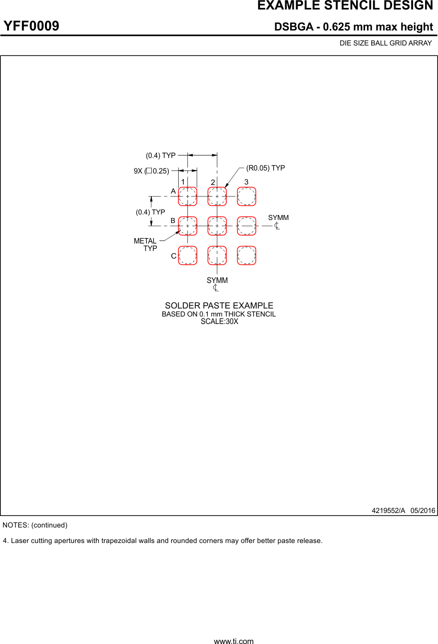
TPS61253 TPS61254 TPS61256 TPS61258 TPS61259 TPS612592 YFF0009_4219552_Page_03.gif