JAJSEX9A July   2011  – March 2018 TPS61256A

PRODUCTION DATA.  

  1. 特長
  2. アプリケーション
  3. 概要
    1.     Device Images
      1.      最小のソリューション・サイズのアプリケーション
      2.      効率と負荷電流との関係
  4. 改訂履歴
  5. Pin Configuration and Functions
    1.     Pin Functions
  6. Specifications
    1. 6.1 Absolute Maximum Ratings
    2. 6.2 ESD Ratings
    3. 6.3 Recommended Operating Conditions
    4. 6.4 Thermal Information
    5. 6.5 Electrical Characteristics
    6. 6.6 Typical Characteristics
  7. Parameter Measurement Information
  8. Detailed Description
    1. 8.1 Overview
    2. 8.2 Softstart
    3. 8.3 Undervoltage Lockout
    4. 8.4 Thermal Regulation
    5. 8.5 Thermal Shutdown
    6. 8.6 Functional Block Diagram
    7. 8.7 Feature Description
      1. 8.7.1 Power-Save Mode
      2. 8.7.2 Current Limit Operation
      3. 8.7.3 Enable
      4. 8.7.4 Load Disconnect And Reverse Current Protection
    8. 8.8 Device Functional Modes
      1. 8.8.1 Load Disconnect And Reverse Current Protection
      2. 8.8.2 Softstart
      3. 8.8.3 Undervoltage Lockout
      4. 8.8.4 Thermal Regulation
      5. 8.8.5 Thermal Shutdown
  9. Application and Implementation
    1. 9.1 Application Information
    2. 9.2 Typical Application
      1. 9.2.1 Design Requirements
      2. 9.2.2 Detailed Design Procedure
        1. 9.2.2.1 Inductor Selection
          1. 9.2.2.1.1 High-frequency Converter Applications
        2. 9.2.2.2 Output Capacitor
        3. 9.2.2.3 Input Capacitor
        4. 9.2.2.4 Checking Loop Stability
      3. 9.2.3 Application Curves
  10. 10Power Supply Recommendations
  11. 11Layout
    1. 11.1 Layout Guidelines
    2. 11.2 Layout Example
    3. 11.3 Thermal Information
  12. 12Package Summary
    1. 12.1 Package Dimensions
  13. 13デバイスおよびドキュメントのサポート
    1. 13.1 デバイス・サポート
      1. 13.1.1 デベロッパー・ネットワークの製品に関する免責事項
    2. 13.2 ドキュメントの更新通知を受け取る方法
    3. 13.3 コミュニティ・リソース
    4. 13.4 商標
    5. 13.5 静電気放電に関する注意事項
    6. 13.6 Glossary
  14. 14メカニカル、パッケージ、および注文情報

パッケージ・オプション

デバイスごとのパッケージ図は、PDF版データシートをご参照ください。

メカニカル・データ(パッケージ|ピン)
  • YFF|9
サーマルパッド・メカニカル・データ
発注情報

Current Limit Operation

The TPS61256A device employs a valley current limit sensing scheme. Current limit detection occurs during the off-time by sensing of the voltage drop across the synchronous rectifier.

The output voltage is reduced as the power stage of the device operates in a constant current mode. The maximum continuous output current (IOUT(CL)), before entering current limit (CL) operation, can be defined by Equation 1.

Equation 1. TPS61256A eq1_IOUT_DD_lvsag8.gif

The duty cycle (D) can be estimated by Equation 2

Equation 2. TPS61256A eq2_D_DD_lvs956.gif

and the peak-to-peak current ripple (ΔIL) is calculated by Equation 3

Equation 3. TPS61256A eq3_diL_DD_lvs956.gif

The output current, IOUT(DC), is the average of the rectifier ripple current waveform. When the load current is increased such that the lower peak is above the current limit threshold, the off-time is increased to allow the current to decrease to this threshold before the next on-time begins (so called frequency fold-back mechanism). When the current limit is reached the output voltage decreases during further load increase.

illustrates the inductor and rectifier current waveforms during current limit operation.
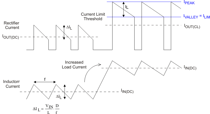
TPS61256A ind_cur_lvsag8.gifFigure 13. Inductor/Rectifier Currents In Current Limit Operation