SLVS978D March 2010 – September 2016 TPS61310 , TPS61311
PRODUCTION DATA.
- 1 Features
- 2 Applications
- 3 Description
- 4 Revision History
- 5 Device Comparison Table
- 6 Pin Configuration and Functions
- 7 Specifications
- 8 Parameter Measurement Information
-
9 Detailed Description
- 9.1 Overview
- 9.2 Functional Block Diagram
- 9.3
Feature Description
- 9.3.1 Privacy Indicator
- 9.3.2
Safe Operation and Protection Features
- 9.3.2.1 LED Temperature Monitoring (Finger-Burn Protection)
- 9.3.2.2 LED Failure Modes (Open and Short Detection) and Overvoltage Protection
- 9.3.2.3 LED Current Ramp-Up and Ramp-Down
- 9.3.2.4 Battery Voltage Droop Monitoring and Protection
- 9.3.2.5 Undervoltage Lockout
- 9.3.2.6 Hot Die Detection and Thermal Shutdown
- 9.3.2.7 Current Limit
- 9.3.2.8 Flash Blanking (Tx-Mask) for Instantaneous Flash Current Reduction
- 9.3.3 Start-Up Sequence
- 9.3.4 NRESET Input: Hardware Enable or Disable
- 9.3.5 Serial Interface Description
- 9.3.6 LED Forward Voltage Calibration
- 9.4 Device Functional Modes
- 9.5 Register Maps
- 10Application and Implementation
- 11Power Supply Recommendations
- 12Layout
- 13Device and Documentation Support
- 14Mechanical, Packaging, and Orderable Information
9 Detailed Description
9.1 Overview
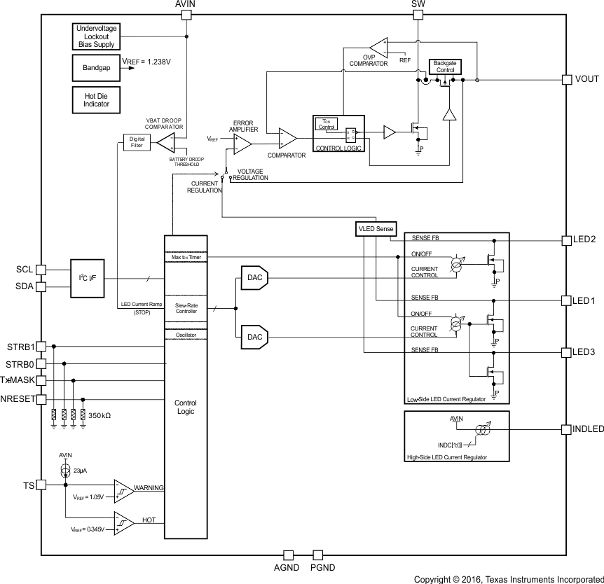
The TPS6131x family is an integrated solution with a wide feature set for driving up to three LEDs for still-camera flash and video-camera lighting applications. It employs a 2-MHz fixed on-time, PWM current-mode converter to generate the output voltage required to drive up to three high-power LEDs in parallel. The device integrates an NMOS-switch power stage and a synchronous PMOS rectifier. The device also implements a set of linear low-side current regulators to control the LED current when the battery voltage is higher than the diode forward voltage.
The high-efficiency boost converter stage and LED forward voltage adoption ensure lowest device input current for a given LED output current.
A special circuit disconnects the load from the battery during shutdown of the converter. In conventional synchronous-rectifier circuits, the back-gate diode of the high-side PMOS is forward biased in shutdown, allowing current to flow from the battery to the output. The TPS6131x prevents this by disconnecting the cathode of the back-gate diode of the high-side PMOS from the source when the regulator is in shutdown.
The TPS6131x device not only operates as a regulated current source, but also as a standard voltage-boost regulator featuring a power-save mode for improved efficiency at light loads. If the input voltage is higher than the programmed output voltage, a down mode is implemented that acts similarly to an LDO.
The power stage is capable of supplying a maximum total current of roughly 1500 mA. The TPS6131x provides three constant-current sinks, capable of sinking up to 2 × 400 mA (LED1 and LED3) and 800 mA (LED2) in flash mode.
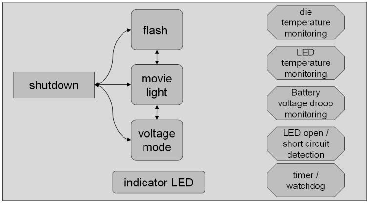 Figure 25. TPS6131x States
Special effort is taken for safe operation and robust system integration. The battery voltage can be monitored so that the flash current is not increased if the battery voltage drops by a programmable threshold. Internal timers limit the flash ON time to prevent potential camera-engine software errors, and a video light watchdog acts in a similar fashion. Multiple monitoring features (LED and die temperature, input voltage droop and so forth) keep the device and LEDs operating properly.
The TPS6131x integrates an I2C compatible interface allowing transfers up to 3.4 Mbps for controlling the device, featuring low-speed mode, standard mode and high-speed mode compatible operation. Additionally, basic functions can be triggered by dedicated hardware input signals, such as STRB0 and STRB1 for triggering the flash or video lighting with zero latency.
9.2 Functional Block Diagram
9.3 Feature Description
9.3.1 Privacy Indicator
The privacy indicator functionality can be used to indicate when a person is being photographed or filmed. The TPS6131x device offers two options of privacy indication: A dedicated pin driving an additional privacy indicator LED or using the white LEDs with pulse width modulation.
9.3.1.1 Dedicated LED Privacy Indicator
The TPS6131x device provides a high-side linear constant current source to drive low VF LEDs. The LED current is directly regulated off the battery and can be controlled through the INDC[3:0] bits, from 2.6 mA to 15.8 mA in 7 programable current steps.
The device can drive two possible hardware configurations shown in Figure 28 and Figure 29. In Figure 28 the TPS6131x device drives a privacy indicator LED towards ground.
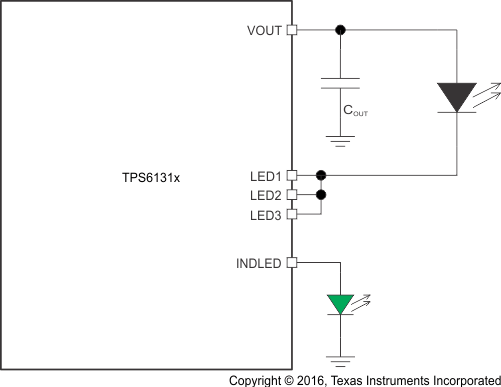 Figure 28. Configuration 1
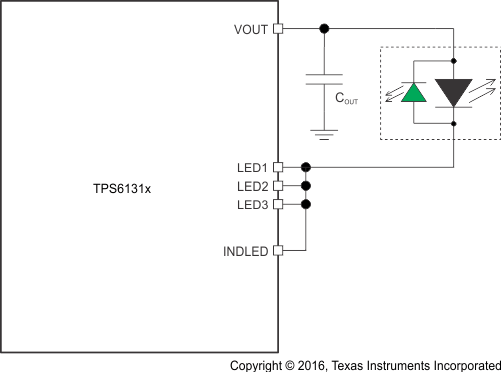 Figure 29. Configuration 2
The TPS6131x device also allows a path for driving a privacy indicator LED that is reverse biased to the white flash LED, see Figure 29. To do so, the output of the converter (VOUT) is pulled to ground thus allowing a reverse current to flow. This mode of operation is only possible when the converter’s power stage is in shutdown (MODE_CTRL[1:0] = 00, ENVM = 0).
9.3.1.2 White LED Privacy Indicator
The TPS6131x device features white LED drive capability at very low light intensity. To generate a reduced LED average current, the device employs a 30-kHz fixed-frequency PWM modulation scheme. The PWM timer uses the internal oscillator as reference clock, therefore the PWM modulating frequency shows the same accuracy as the internal reference clock. Operation is shown in Figure 27.
The video light current is modulated with a duty cycle defined by the INDC[3:0] bits. The low light dimming mode can only be activated in the software-controlled video-light-only mode (MODE_CTRL[1:0] = 01, ENVM = 1), and applies to the LEDs selected through ENLED[3:1] bits. In this mode, the video light safety-timeout feature is disabled.
 Figure 30. PWM Dimming Principle
9.3.2 Safe Operation and Protection Features
9.3.2.1 LED Temperature Monitoring (Finger-Burn Protection)
The TPS6131x device optionally monitors the LED temperature. Critical temperatures are handled in two stages reflected by two bits: LEDWARN provides an early warning to the camera engine, LEDHOT immediately suspends the flash operation.
The LED temperature is sensed by measuring the voltage drop of a negative-temperature-coefficient resistor connected between the TS and AGND pins. An internal current source provides the bias (approximately 24 µA) for the NTC, and the TS pin voltage is compared to internal thresholds (1.05 V and 0.345 V) to protect the LEDs against overheating. See NTC Selection.
The temperature-monitoring blocks are explicitly active in video light or flash modes. In voltage-mode operation [MODE_CTRL[1:0] = 11], the device only activates the TS input when the ENTS bit is set high.
The LEDWARN and LEDHOT bits reflect the LED temperature. The LEDWARN bit is set when the voltage at the TS pin is lower than 1.05 V. This threshold corresponds to an LED warning temperature value; device operation is still permitted. While regulating LED current, video light or flash modes, the LEDHOT bit is latched when the voltage at the TS pin is lower than 0.345 V. This threshold corresponds to an excessive LED temperature value; device operation is immediately suspended, (MODE_CTRL[1:0] bits are reset, and the HOTDIE[1:0] bits are set).
9.3.2.2 LED Failure Modes (Open and Short Detection) and Overvoltage Protection
The TPS6131x devices incorporate protection features to indicate if the connected LEDs are failing. These protections cover overvoltage conditions, which are caused by a failing LED showing open circuit behavior, as well as short-circuit conditions caused by a failing LED or further reasons causing a short-circuit condition. If such failure conditions occur, these are indicated by setting a failure detection flag. Furthermore, the maximum current drawn from the output is limited and can be programmed by the current-limit setting.
9.3.2.2.1 LED Open Circuit Detection and Overvoltage Protection
If the connected LED(s) fail showing an open circuit behavior or are disconnected, the VOUT output voltage must be limited to prevent the step-up converter from exceeding critical values. An overvoltage protection is implemented to avoid the output voltage exceeding critical values for the device and possibly for the system it is supplying. For this protection the TPS6131x output voltage is monitored internally. The TPS6131x device limits VOUT according to the overvoltage protection settings (see Table 2). In this failure mode, VOUT is either limited to 4.65 V (typical) or 6 V (typical) and the HIGH-POWER LED FAILURE (HPLF) flag is set. The OVP threshold depends on the programmed output voltage (OV).
Table 2. OVP Specification
| OVP THRESHOLD | OPERATING CONDITIONS |
|---|---|
| 4.65 V typical | 0000 ≤ OV[3:0] ≤ 0100 |
| 6 V typical | 0101 ≤ OV[3:0] ≤ 1111 |
9.3.2.2.2 Short-Circuit Protection
The TPS6131x devices incorporate double protection to protect the device and application circuit from short-circuit conditions occurring between VOUT and the current sinks LED1, LED2, and LED3.
If a short-circuit condition occurs while the LEDs are operated, the low side current sinks LED1, LED2, LED3 limit the maximum output current as programmed for the video-light mode or flash mode respectively. If a short-circuit condition occurs, the current sinks increase their input resistance to prevent excessive current to be drawn. Furthermore, the HIGH-POWER LED FAILURE flag (HPLF) is set to indicate the short circuit condition. (HPLF) is triggered if the LED forward voltage drops below 1.23 V typically. The second protection is the current limit, which generally limits the current drawn from VOUT. See Current Limit.
9.3.2.3 LED Current Ramp-Up and Ramp-Down
To achieve smooth LED current waveforms and avoid excessive battery voltage drop, the TPS6131x device actively controls the LED current ramp-up and ramp-down sequence.
Table 3. LED Current Ramp-Up and Ramp-Down Control vs Operating Mode
| LED CURRENT | OPERATING MODE |
|---|---|
| Ramp-up | ISTEP = 25 mA |
| tRISE = 12 µs | |
| Slew rate × 2.1 mA/µs | |
| Ramp-down | ISTEP = 25 mA |
| tFALL = 0.5 µs | |
| Slew rate × 50 mA/µs |
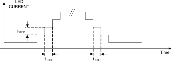 Figure 31. LED Current Slew Rate Control
9.3.2.4 Battery Voltage Droop Monitoring and Protection
During a high-power flash strobe, the battery voltage usually drops by a few hundred millivolts. To prevent the battery voltage from collapsing too much, the TPS6131x devices integrates a battery voltage droop monitoring feature to automatically limit the flash current if the battery voltage drops more than a programmable threshold.
The battery voltage droop monitoring feature can be enabled or disabled through the ENBATMON bit.
At the very beginning of the flash strobe, the device measures the battery voltage and sets a minimum battery voltage threshold based on the tolerable droop (see REGISTER7 (address = 0x07) for BATDROOP[2:0] bits). While the LED current is increasing to the target flash current (see REGISTER1 (address = 0x01) and REGISTER2 (address = 0x02) for FC13[4:0] and FC2[5:0] bits), a comparator monitors the actual battery voltage and stops the ramp-up sequence when the droop exceeds the limit. See Functional Block Diagram and Figure 32.
The battery voltage droop monitor feature is automatically disabled during a Tx-MASK event.
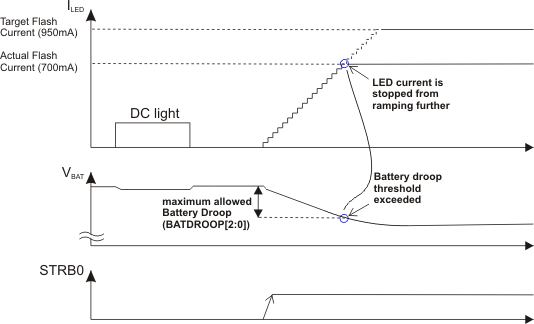 Figure 32. Battery Voltage Droop Monitoring and LED Current Control Principle (STRB1 = 0, Tx-Base = 1)
9.3.2.5 Undervoltage Lockout
The undervoltage lockout circuit prevents the device from error conditions at low input voltages. It prevents the converter from turning on the switch MOSFET, or rectifier MOSFET for battery voltages below 2.3 V. The I2C compatible interface is fully functional down to 2.1-V input voltage.
9.3.2.6 Hot Die Detection and Thermal Shutdown
The TPS6131x device offers two levels of die temperature monitoring and protection, which are hot die detection and thermal shutdown functionality. The hot die detector (HOTDIE[1:0] bits) reflects the instantaneous junction temperature. This functionality is always enabled except when the device is in shutdown mode.
The hot die detector monitors the junction temperature but does not shut down the device. It provides an early warning to the camera engine to avoid excessive power dissipation thus preventing from thermal shutdown during the next high-power flash strobe.
As soon as the junction temperature TJ exceeds 160°C typical, the device goes into thermal shutdown. In this mode, the power stage and the low-side current regulators are turned off, the HOTDIE[1:0] bits are set and can only be reset by a read access. In the voltage mode operation (MODE_CTRL[1:0] = 11 or ENVM = 1), the device continues its operation when the junction temperature falls below 140°C typical again. In the current regulation mode, video light or flash modes, device operation is suspended.
Table 4. Die Temperature Bits
| HOTDIE[1:0] | JUNCTION TEMPERATURE |
|---|---|
| 00 | <55°C |
| 01 | 55°C ≤ TJ ≤ 70°C |
| 10 | >70°C |
| 11 | Thermal shutdown tripped. The bit is reset after read access |
9.3.2.7 Current Limit
The TPS6131x devices employ a programmable inductor current limit. This allows choosing inductors with different saturation current ratings. Furthermore, this provides protection against a shorted inductor, or if the inductance value dramatically drops. This protects the battery from excessively high current drain.
The current limit circuit employs a valley current sensing scheme. The detection threshold is user selectable through the ILIM bit. The ILIM bit can only be set before entering operation, during initial shutdown state.
Figure 33 illustrates the inductor and rectifier current waveforms during current limit operation. The output current, IOUT, is the average of the rectifier ripple current waveform. When the load current is increased such that the lower peak is above the current limit threshold, the off time is lengthened to allow the current to decrease to this threshold before the next ON time begins (so called frequency foldback mechanism).
Both the output voltage and the switching frequency are reduced as the power stage of the device operates in a constant current mode. The maximum continuous output current (IOUT(CL)), before entering current limit operation, can be defined as:

The TPS6131x device also provides a negative current limit (≈ 300 mA) to prevent an excessive reverse inductor current when the power stage sinks current from the output in the forced continuous conduction mode.
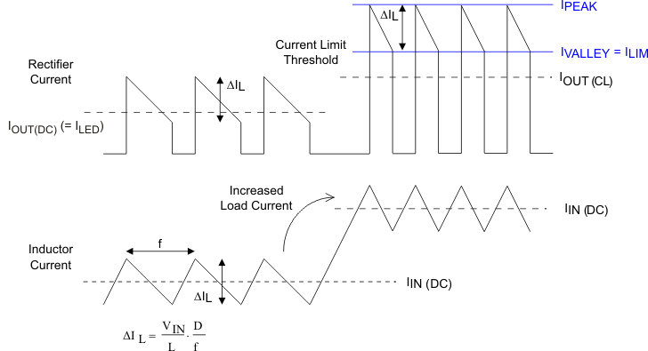 Figure 33. Inductor and Rectifier Currents in Current Limit Operation
Table 5. Inductor Current Limit Operation
| CURRENT LIMIT SETTING | ILIM BIT | |
|---|---|---|
| TPS61310 | TPS61311 | |
| 1250 mA | 1800 mA | Low |
| 1750 mA | 2480 mA | High |
9.3.2.8 Flash Blanking (Tx-Mask) for Instantaneous Flash Current Reduction
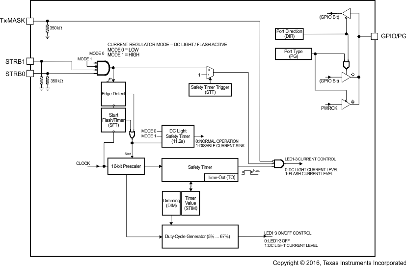
The TPS6131x devices offer a dedicated hardware signal input (Tx-Mask) that can be used to reduce the flash current to the programmed video light level instantaneously.
This feature can be used to reduce the overall current drawn from the battery if other system components require high energy simultaneously, such as during a RF PA transmission pulse.
The Tx-MASK function has no influence on the safety timer duration.
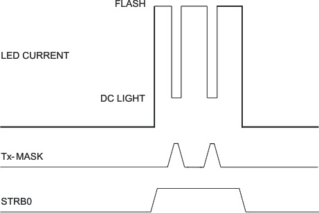 Figure 34. Synchronized Flash With Blanking Periods (STRB1 = 0)
9.3.3 Start-Up Sequence
To avoid high inrush current during start-up, control the inrush current. When the device enables, the internal start-up cycle starts with the first step, the precharge phase.
During precharge, the rectifying switch is turned on until the output capacitor is either charged to a value close to the input voltage or ≈ 3.3 V, whichever occurs first. The rectifying switch is current limited during that phase. The current limit increases with decreasing input-to-output voltage difference. This circuit also limits the output current under output short-circuit conditions.
After precharging the output capacitor, the device starts switching, and increases its current limit in three steps of typically 25 mA, 250 mA and full current limit (ILIM setting). The current limit transition from the first to the second step occurs after 1 ms of operation. Full current limit operation is set once the output voltage reaches its regulation limits. In this mode, the active balancing circuit is disabled.
9.3.4 NRESET Input: Hardware Enable or Disable
The TPS6131x family features a hardware reset pin (NRESET). This reset pin allows the device to be disabled by an external controller without requiring an I2C write command. Under normal operation, the NRESET pin must be held high to prevent an unwanted reset. When the NRESET is driven low, the I2C control interface and all internal control registers are reset to the default states and the part enters shutdown mode.
9.3.5 Serial Interface Description
I2C™ is a 2-wire serial interface developed by Philips Semiconductor, now NXP Semiconductors [1]. The bus consists of a data line (SDA) and a clock line (SCL) with pullup structures. When the bus is idle, both SDA and SCL lines are pulled high. All the I2C compatible devices connect to the I2C bus through open drain I/O pins, SDA and SCL. A master device, usually a microcontroller or a digital signal processor, controls the bus. The master is responsible for generating the SCL signal and device addresses. The master also generates specific conditions that indicate the START and STOP of data transfer. A slave device receives or transmits data on the bus under control of the master device.
The TPS6131x device works as a slave and supports these data transfer modes, as defined in the I2C Bus Specification: standard mode (100 kbps) and fast mode (400 kbps), and high-speed mode (3.4 Mbps). The interface adds flexibility to the power supply solution, enabling most functions to be programmed to new values depending on the instantaneous application requirements. Register contents remain intact as long as supply voltage remains above 2.1 V.
The data transfer protocol for standard and fast modes is exactly the same, therefore they are referred to as F/S-mode in this document. The protocol for high-speed mode is different from F/S-mode, and it is referred to as H/S-mode. The TPS6131x device supports 7-bit addressing; 10-bit addressing and general call address are not supported. The device 7-bit address is defined as 011 0011.
9.3.5.1 F/S-Mode Protocol
The master initiates data transfer by generating a start condition. The start condition is when a high-to-low transition occurs on the SDA line while SCL is high, as shown in Figure 35. All I2C-compatible devices must recognize a start condition.
 Figure 35. Start and Stop Conditions
The master then generates the SCL pulses, and transmits the 7-bit address and the read or write direction bit (R/W) on the SDA line. During all transmissions, the master checks for valid data. A valid data condition requires the SDA line to be stable during the entire high period of the clock pulse (see Figure 36). All devices recognize the address sent by the master and compare it to their internal fixed addresses. Only the slave device with a matching address generates an acknowledge (see Figure 37) by pulling the SDA line low during the entire high period of the ninth SCL cycle. Upon detecting this acknowledge, the master knows that communication link with a slave has been established.
 Figure 36. Bit Transfer on the Serial Interface
The master generates further SCL cycles to either transmit data to the slave (R/W bit 1) or receive data from the slave (R/W bit 0). In either case, the receiver must to acknowledge the data sent by the transmitter. So an acknowledge signal can either be generated by the master or by the slave, depending on which one is the receiver. 9-bit valid data sequences consisting of 8-bit data and 1-bit acknowledge can continue as long as necessary.
To signal the end of the data transfer, the master generates a stop condition by pulling the SDA line from low to high while the SCL line is high (see Figure 35). This releases the bus and stops the communication link with the addressed slave. All I2C compatible devices must recognize the stop condition. Upon the receipt of a stop condition, all devices know that the bus is released, and they wait for a start condition followed by a matching address.
Attempting to read data from register addresses not listed in this section results in 00h being read out.
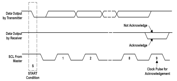 Figure 37. Acknowledge on the I2C Bus
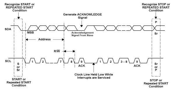 Figure 38. Bus Protocol
9.3.5.2 H/S-Mode Protocol
The master generates a start condition followed by a valid serial byte containing HS master code 00001XXX. This transmission is made in F/S-mode at no more than 400 Kbps. No device is allowed to acknowledge the HS master code, but all devices must recognize it and switch their internal setting to support 3.4-Mbps operation.
The master then generates a repeated start condition (a repeated start condition has the same timing as the start condition). After this repeated start condition, the protocol is the same as F/S-mode, except that transmission speeds up to 3.4 Mbps are allowed. A stop condition ends the H/S-mode and switches all the internal settings of the slave devices to support the F/S-mode. Instead of using a stop condition, repeated start conditions should be used to secure the bus in H/S-mode.
Attempting to read data from register addresses not listed in this section results in 00h being read out.
9.3.5.3 TPS6131x I2C Update Sequence
The TPS6131x requires a start condition, a valid I2C address, a register address byte, and a data byte for a single update. After the receipt of each byte, TPS6131x device acknowledges by pulling the SDA line low during the high period of a single clock pulse. A valid I2C address selects the TPS6131x. TPS6131x performs an update on the falling edge of the acknowledge signal that follows the LSB byte.
 Figure 39. : Write Data Transfer Format in F/S-Mode
 Figure 40. Read Data Transfer Format in F/S-Mode
 Figure 41. Data Transfer Format in H/S-Mode
9.3.5.4 Slave Address Byte
| MSB | LSB | ||||||
|---|---|---|---|---|---|---|---|
| X | X | X | X | X | X | A1 | A0 |
The slave address byte is the first byte received following the START condition from the master device.
9.3.5.5 Register Address Byte
| MSB | LSB | ||||||
|---|---|---|---|---|---|---|---|
| 0 | 0 | 0 | 0 | 00 | D2 | D1 | D0 |
Following the successful acknowledgment of the slave address, the bus master sends a byte to the TPS6131x, which contains the address of the register to be accessed.
9.3.6 LED Forward Voltage Calibration
High-power LEDs tend to exhibit a wide forward voltage distribution. The TPS6131x device integrates a self-calibration procedure that can be used to determine the actually LED forward voltage. The LED forward voltage in situ characterization can be performed at camera engine production test. This data can help to estimate more precisely the actual LED electrical power versus flash current.
This calibration procedure is meant to start at a minimum output voltage, and can be initiated by writing the SELFCAL bit (preferably with MODE_CTRL[1:0] = 00, ENVM = 0). The calibration procedure monitors the sense voltage across the low-side current regulators (according to ENLED[3:1] bits setting) and registers the worst case LED, the LED featuring the largest forward voltage. The TPS6131x device automatically sweeps through its output voltage range and performs a short duration flash strobe for each step (see REGISTER1 (address = 0x01) and REGISTER2 (address = 0x02) for FC13[4:0] and FC2[5:0] bits settings).
The sequence is stopped as soon as the device detects that each of the low-side current regulators have enough headroom voltage (400 mV typical). The device returns the according output voltage in the register OV[3:0] and sets the SELFCAL bit. This bit is only being reset at the start or restart of a calibration cycle. In other words, when SELFCAL is asserted the output voltage register (OV[3:0]) returns the result of the last calibration sequence.
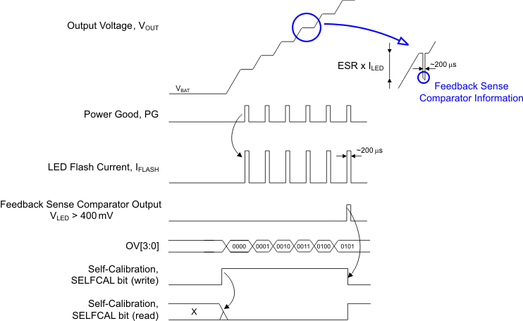 Figure 42. LED Forward Voltage Calibration Principle
9.4 Device Functional Modes
9.4.1 Video Light and Flash Strobe Operation
The TPS6131x devices drive one, two or three LEDs for video light and flash application. The video light and flash operation can either be triggered by an I2C software command or by means of dedicated, zero latency hardware signals.
9.4.1.1 LED Hardware Setup
The TPS6131x device uses LED forward-voltage sensing circuitry on LED1, LED2, and LED3 pins to optimize the power-stage boost ratio for maximum efficiency. Due to the nature of the sensing circuitry, TI does not recommend leaving any of the LED1, LED2, and LED3 pins unused if the operation is selected through ENLED[3:1] bits. Leaving LED1, LED2, and LED3 pins unconnected, while the respective ENLEDx bits have been set, forces the control loop into high gain, and eventually trips the output overvoltage protection. Figure 43 shows the recommended LED setup for a single, dual or triple-LED application.
 Figure 43. White LED Hardware Setup Options
The LED1, LED2, and LED3 inputs may be connected together to drive one or two LEDs at higher currents. Connecting the current sink inputs in parallel does not affect the internal operation of the TPS6131x. For best operation, TI recommends disabling the LED inputs that are not connected. (see the ENLED[3:1] bits description in REGISTER5 (address = 0x05)).
The video light currents are individually programmed through the video light control bits DCL13[2:0] and DCL2[2:0] , the flash currents through FC2[5:0] and FC13[4:0] bits accordingly. If, for single or dual LED application as shown in Figure 43, current sinks are connected to each other and enabled, the resulting video or flash current is the sum of the programmed currents.
9.4.1.2 Triggering Video Light and Flash
For most flexible system integration, the TPS6131x offers several options for activating the video light and flash. Depending on the settings of the MODE_CTRL[1:0] bits, the device can enter different modes of operation. It offers the option of triggering the video light and flash through hardware signals (STRB0, STRB1) or software I2C command. The flash-signal hardware trigger can be on the leading-edge, turning on for the programmed flash on time, or level sensitive, turning on for as long as the signal is logic high.
The TPS6131x flash timer is programmed through the STIM[2:0] and SELSTIM bits. If the flash is fired by a rising-edge trigger or by an I2C command, the timer defines the flash duration. If the flash is fired by a level-sensitive trigger, the timer defines the maximum flash ON duration, and overrides the hardware signal if the programmed on-time is exceeded.
For video lighting, a watchdog timer is implemented; this must be refreshed within 13 seconds. This function can be disabled, as described in Table 6.
Table 6. Mode Operations for Video Light and Flash
| MODE_CTRL SETTING | DESCRIPTION |
|---|---|
| MODE_CTRL[1:0] = 01 | The STRB0, STRB1 inputs are disabled. The device regulates the LED current in video light mode (DCLC bits) regardless of the STRB0, STRB1 inputs and the START_FLASH/TIMER (SFT) bit. To avoid device shutdown because of the video light safety timeout, MODE_CTRL[1:0] must be refreshed within less than 13 seconds (STRB1 = 0). The video light watchdog timer can be disabled by pulling the STRB1 signal high. |
| MODE_CTRL[1:0] = 10 | The STRB0, STRB1 inputs are enabled. The flash pulse can be triggered by these synchronization signals, or by a software command (START_FLASH/TIMER (SFT) bit). The LEDs are enabled or disabled according to the STRB0, STRB1 input. The flash safety timer is activated, and the video light watchdog timer is disabled. |
The dual-wire camera-module interface STRB0 and STRB1 inputs are used for selecting the video light (STRB1 = 1) or flash (STRB1 = 0) mode. The STRB0 signal then triggers the video light or flash, depending on the state of STRB1. The STT bit defines if the flash trigger is level sensitive (STT = 0), or fired on the rising edge (STT = 1).
9.4.1.3 Level-Sensitive Flash Trigger (STT = 0)
In this mode, the high-power LEDs are driven at the flash current level and the safety timer (STIM) is running. The maximum duration of the flash pulse is defined in the STIM[2:0] register.
The safety timer is triggered on rising edge and stopped by a negative logic on the synchronization source (STRB0, STRB1 = 0) or by a timeout event (TO bit).
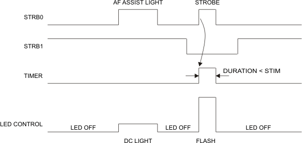 Figure 44. Hardware Synchronized Video Light and Flash Strobe
9.4.1.4 Rising-Edge Flash Trigger (STT = 1)
In this mode, the high-power LEDs are driven at the flash current level and the safety timer (STIM) is running. The duration of the flash pulse is defined in the STIM[2:0] register.
The flash strobe is started either by a rising edge on the synchronization source (STRB0 = 1, STRB1 = 0) or by a positive transition on the START-FLASH/TIMER (SFT) bit (STRB0 = 1, STRB1 = 0). Once running, the timer ignores all kind of triggering signals and only stops after a timeout (TO). START-FLASH/TIMER (SFT) bit is being reset by the timeout (TO) signal.
 Figure 45. Edge Sensitive Timer (Single Trigger Event)
9.4.2 Voltage Mode
In this mode, the TPS6131x operates as a standard voltage-boost regulator, featuring power-save mode for improved efficiency under light loads. The voltage-mode operation is enabled by software control by setting the mode-control bit MODE_CTRL[1:0] = 11. The device regulates a constant output voltage according to the OV[3:0] bit settings (from 3.825 V to 5.7 V in 125-mV steps). In voltage mode, the LED current sinks LED1, LED2, and LED3 are turned off.
The TPS6131x integrates a software control bit (ENVM bit) that can be used to force the converter to run in voltage mode. This enables the converter to operate at a fixed programmed output voltage (according to the OV[3:0] settings) while operating the LEDs.
Table 7 provides an overview of the different voltage mode variations.
Table 7. Voltage Mode Description
| INTERNAL REGISTER SETTINGS MODE_CTRL[1:0] | ENVM BIT | OPERATING MODES |
|---|---|---|
| 11 | 0 | LEDs are turned off and the converter operate in voltage-regulation mode (VM); the output voltage is set through register OV[3:0]. |
| 00 | 1 | |
| 01 | 1 | The converter operates in voltage-regulation mode (VM); the output voltage is set through the register OV[3:0]. The LEDs are turned on for video light operation and the energy is being directly transferred from the battery to the output. The LED currents are regulated by the means of the low-side current sinks. |
| 10 | 1 | The converter operates in the voltage-regulation mode (VM); the output voltage is set through the register OV[3:0]. The LED currents are regulated by the low-side current sinks. The LEDs are ready for flash operation. |
| 11 | 1 | LEDs are turned off and the converter operates in the voltage regulation mode (VM); the output voltage is set through the register OV[3:0]. |
9.4.2.1 Down Mode in Voltage Mode Operation
In general, a boost converter only regulates output voltages which are higher than the input voltage. The TPS6131x can regulate 4.2 V at the output with an input voltage as high as 5.5 V. To control these applications properly, a down-conversion mode is implemented.
In voltage-regulation mode, if the input voltage reaches or exceeds the output voltage, the converter changes to down-conversion mode. In this mode, the control circuit changes the behavior of the rectifying PMOS. It sets the voltage drop across the PMOS as high as required to regulate the output voltage. This increases the power losses in the converter, and must be considered for thermal design. The down-conversion mode is automatically turned off as soon as the input voltage falls to approximately 200 mV below the output voltage.
For proper operation in down-conversion mode the output voltage must not be programmed higher than approximately 5.3 V. Take care not to violate the absolute maximum ratings at the SW pins.
9.4.2.2 Power Good Indication
The TPS6131x integrates a Power Good circuit that is activated when the device operates in voltage-regulation mode (MODE_CTRL[1:0] = 11 or ENVM = 1). In shutdown mode (MODE_CTRL[1:0] = 00, ENVM = 0), the GPIO/PG pin state is defined below, according to the GPIOTYPE bit:
Table 8. GPIO/PG State in Shutdown
| GPIOTYPE | GPIO/PG SHUTDOWN STATE |
|---|---|
| 0 | Reset or pulled to ground |
| 1 | Open-drain |
Depending on the GPIO/PG output stage type selection, push-pull or open-drain, the polarity of the Power Good output signal (PG) can be inverted or not. The Power Good software bit and hardware signal polarity is defined below:
Table 9. Power Good Signal Polarity
| GPIOTYPE | PG BIT | GPIO/PG OUTPUT PORT | COMMENTS |
|---|---|---|---|
| 0: push-pull output | 0 | 0 | Output is active-high |
| 1 | 1 | ||
| 1: open-drain output | 0 | Open-drain | Output is active-low |
| 1 | Low |
The Power Good signal is true when the output voltage is from –1.5% to 2.5% of its nominal value. Conversely, it is false when the voltage-mode operation is suspended (MODE_CTRL[1:0] ≠ 11 and ENVM = 0).
 Figure 46. Power Good Operation (DIR = 1, GPIOTYPE = 1)
The TPS6131x device uses a control architecture that recycles excess energy that might be stored in the output capacitor. By reversing the operation of the boost power stage, the converter is capable of transferring energy from its output back into the input source. In this case, the Power Good signal is deasserted while the output voltage is decreasing towards its target value, the closest fit voltage the converter can support.
9.4.3 Power-Save Mode Operation, Efficiency
The TPS6131x integrates a power-save mode to improve efficiency under light loads. In power-save mode the converter only operates when the output voltage trips below a set threshold voltage. It ramps up the output voltage with one to several pulses and returns to power-save mode once the output voltage exceeds the set threshold voltage.
The power-save mode can be enabled and disabled through the ENPSM bit. In down conversion mode, power-save mode is always active and the device cannot be forced into fixed frequency operation at light loads.
The LED sense voltage has a direct effect on converter efficiency. Because the voltage across the low-side current regulator does not contribute to the output power (LED brightness), the lower the sense voltage the higher the efficiency is.
The integrated current control loop automatically selects the minimum boost ratio to maintain regulation based on the LED forward voltage and current requirements. The low-side current regulators drop the voltage difference between the input voltage and the LEDs forward voltage
(VF(LED) < VIN). When running in boost mode (VF(LED) > VIN), the voltage present at the LED1, LED2, and LED3 pins of the low-side current regulators is typically 400 mV, leading to high power conversion efficiency. Depending on the input voltage and the LEDs forward voltage characteristic the converter efficiency is approximately 75% to 90%.
9.4.4 Shutdown
Writing 00 to MODE_CTRL[1:0] bits forces the device into shutdown. The shutdown state can only be entered when the voltage regulation (ENVM = 0) and light modes are both turned off.
In the shutdown state:
- The regulator stops switching.
- The high-side PMOS disconnects the load from the input.
- The LEDx pins are high impedance thus eliminating any DC conduction path.
- The TPS6131x device actively discharges the output capacitor when it turns off.
9.5 Register Maps
9.5.1 REGISTER0 (address = 0x00)
| D7 | D6 | D5 | D4 | D3 | D2 | D1 | D0 |
| RESET | — | DCLC13[2:0] | DCLC2[2:0] | ||||
| R/W-0 | R/W-0 | R/W-0 | R/W-0 | R/W-1 | R/W-0 | R/W-1 | R/W-0 |
Table 10. REGISTER0 Field Descriptions
| BIT | DESCRIPTION |
|---|---|
| RESET | Register Reset bit
0: Normal operation. 1: Default values are set to all internal registers. |
| DCLC13[2:0] | Video Light Current Control bits (LED1 and LED3)
000: 0 mA(1)(2) 001: 25 mA 010: 50 mA 011: 75 mA 100: 100 mA 101: 125 mA 110: 150 mA 111: 175 mA |
| DCLC2[2:0] | Video Light Current Control bits (LED2)
000: 0 mA(1)(2) 001: 25 mA 010: 50 mA 011: 75 mA 100: 100 mA 101: 125 mA 110: 150 mA, 225 mA current level can be activated simultaneously with Tx-MASK = 1 111: 175 mA, 325 mA current level can be activated simultaneously with Tx-MASK = 1 |
9.5.2 REGISTER1 (address = 0x01)
| D7 | D6 | D5 | D4 | D3 | D2 | D1 | D0 |
| MODE_CTRL[1:0] | FC2[5:0] | ||||||
| R/W-0 | R/W-0 | R/W-0 | R/W-1 | R/W-0 | R/W-0 | R/W-0 | R/W-0 |
Table 11. REGISTER1 Field Descriptions
| BIT | DESCRIPTION |
|---|---|
| MODE_CTRL[1:0] | Mode Control bits
00: Device in shutdown mode. 01: Device operates in video light mode. 10: Device operates in flash mode. 11: Device operates as constant voltage source. To avoid device shutdown by video light safety timeout, MODE_CTRL[1:0] bits must be refreshed within less than 13 s. Writing to REGISTER1[7:6] automatically updates REGISTER2[7:6]. |
| FC2[5:0] | Flash Current Control bits (LED2)
000000: 0 mA(1)(2) 000001: 25 mA 000010: 50 mA 000011: 75 mA 000100: 100 mA 000101: 125 mA 000110: 150 mA 000111: 175 mA 001000: 200 mA 001001: 225 mA 001010: 250 mA 001011: 275 mA 001100: 300 mA 001101: 325 mA 001110: 350 mA 001111: 375 mA 010000: 400 mA 010001: 425 mA 010010: 450 mA 010011: 475 mA 010100: 500 mA 010101: 525 mA 010110: 550 mA 010111: 575 mA 011000: 600 mA 011001: 625 mA 011010: 650 mA 011011: 675 mA 011100: 700 mA 011101: 725 mA 011110: 750 mA 011111: 775 mA 100000 to 111111: 800 mA |
9.5.3 REGISTER2 (address = 0x02)
| D7 | D6 | D5 | D4 | D3 | D2 | D1 | D0 |
| MODE_CTRL[1:0] | ENVM | FC13[4:0] | |||||
| R/W-0 | R/W-0 | R/W-0 | R/W-0 | R/W-1 | R/W-0 | R/W-0 | R/W-0 |
Table 12. REGISTER2 Field Descriptions
| BIT | DESCRIPTION |
|---|---|
| MODE_CTRL[1:0] | Mode Control bits
00: Device in shutdown mode. 01: Device operates in video light mode. 10: Device operates in flash mode. 11: Device operates as constant voltage source. To avoid device shutdown by video light safety timeout, MODE_CTRL[1:0] bits must be refreshed within less than 13 s. Writing to REGISTER2[6:5] automatically updates REGISTER1[6:5]. |
| ENVM | Enable Voltage Mode bit. 0: Normal operation. 1: Forces the device into a constant voltage source. In read mode, the ENVM bit is automatically updated to reflect the logic state of the ENVM input pin. |
| FC13[4:0] | Flash Current Control bits (LED1 and LED3)
00000: 0 mA(1)(2) 00001: 25 mA 00010: 50 mA 00011: 75 mA 00100: 100 mA 00101: 125 mA 00110: 150 mA 00111: 175 mA 01000: 200 mA 01001: 225 mA 01010: 250 mA 01011: 275 mA 01100: 300 mA 01101: 325 mA 01110: 350 mA 01111: 375 mA 10000 to 11111: 400 mA |
9.5.4 REGISTER3 (address = 0x03)
| D7 | D6 | D5 | D4 | D3 | D2 | D1 | D0 |
| STIM[2:0] | HPFL | SELSTIM (W) TO (R) |
STT | SFT | Tx-MASK | ||
| R/W-1 | R/W-1 | R/W-0 | R-0 | R-0 | R/W-0 | R/W-0 | R/W-1 |
Table 13. REGISTER3 Field Descriptions
| BIT | DESCRIPTION | ||
|---|---|---|---|
| STIM[2:0] | Safety Timer bits | ||
| STIM[2:0]
000 001 010 011 100 101 110 111 |
RANGE 0
68.2 ms 102.2 ms 136.3 ms 170.4 ms 204.5 ms 340.8 ms 579.3 ms 852 ms |
RANGE 1
5.3 ms 10.7 ms 16 ms 21.3 ms 26.6 ms 32 ms 37.3 ms 71.5 ms |
|
| HPFL | High-Power LED Failure flag
0: Proper LED operation. 1: LED failed (open or shorted). High-power LED failure flag is reset after readout |
||
| SELSTIM | Safety Timer Selection Range (Write Only)
0: Safety timer range 0. 1: Safety timer range 1. |
||
| TO | Time-Out Flag (Read Only)
0: No time-out event occurred. 1: Time-out event occurred. Time-out flag is reset at restart of the safety timer. |
||
| STT | Safety Timer Trigger bit
0: LED safety timer is level sensitive. 1: LED safety timer is rising edge sensitive. This bit is only valid for MODE_CTRL[1:0] = 10. |
||
| SFT | Start/Flash Timer bit
In write mode, this bit initiates a flash strobe sequence. Notice that this bit is only active when STRB0 input is high. 0: No change in the high-power LED current. 1: High-power LED current ramps to the flash current level. In read mode, this bit indicates the high-power LED status. 0: High-power LEDs are idle. 1: Ongoing high-power LED flash strobe. |
||
| Tx-MASK | Flash Blanking Control bit
In write mode, this bit enables and disables the flash blanking and LED current reduction function. 0: Flash blanking disabled. 1: LED current is reduced to video light level when Tx-MASK input is high. In read mode, this flag indicates whether or not the flash masking input is activated. Tx-MASK flag is reset after readout of the flag. 0: No flash blanking event occurred. 1: Tx-MASK input triggered. |
||
9.5.5 REGISTER4 (address = 0x04)
| D7 | D6 | D5 | D4 | D3 | D2 | D1 | D0 |
| PG | HOTDIE[1:0] | ILIM | INDC[3:0] | ||||
| R/W-0 | R-0 | R-0 | R/W-0 | R/W-0 | R/W-0 | R/W-0 | R/W-0 |
Table 14. REGISTER4 Field Descriptions
| Bit | Description | |||
|---|---|---|---|---|
| PG | Power Good bit
In write mode, this bit selects the functionality of the GPIO/PG output. 0: PG signal is routed to the GPIO port. 1: GPIO PORT VALUE bit is routed to the GPIO port. In read mode, this bit indicates the output voltage conditions. 0: The converter is not operating within the voltage regulation limits. 1: The output voltage is within its nominal value. |
|||
| HOTDIE[1:0] | Instantaneous Die Temperature bits
00: TJ < 55°C 01: 55°C < TJ < 70°C 10: TJ > 70°C 11: Thermal shutdown tripped. Indicator flag is reset after readout. |
|||
| ILIM | Inductor Valley Current Limit bit
The ILIM bit can only be set before the device enters operation, during initial shutdown state. |
|||
| VALLEY CURRENT LIMIT SETTING | ILIM BIT SETTING | |||
| TPS61310 1250 mA 1750 mA |
TPS61311 1800 mA 2480 mA |
Low High |
||
| INDC[3:0] | Indicator Light Control bits | |||
| INDC[3:0]: PRIVACY INDICATOR INDLED CHANNEL
_ 0000: Privacy indicator turned off 0001: INDLED current = 2.6 mA(1) 0010: INDLED current = 5.2 mA(1) 0011: INDLED current = 7.9 mA(1) 0100: Privacy indicator turned off 0101: INDLED current = 5.2 mA(1) 0110: INDLED current = 10.4 mA(1) 0111: INDLED current = 15.8 mA (1) |
INDC[3:0]: PRIVACY INDICATOR LED1, LED2, and LED3 CHANNELS(2)
1000: 5% PWM dimming ratio 1001: 11% PWM dimming ratio 1010: 17% PWM dimming ratio 1011: 23% PWM dimming ratio 1100: 30% PWM dimming ratio 1101: 36% PWM dimming ratio 1110: 48% PWM dimming ratio 1111: 67% PWM dimming ratio |
|||
9.5.6 REGISTER5 (address = 0x05)
| D7 | D6 | D5 | D4 | D3 | D2 | D1 | D0 |
| SELFCAL | ENPSM | DIR (W) STSTRB1 (R) |
GPIO | GPIOTYPE | ENLED3 | ENLED2 | ENLED1 |
| R/W-0 | R/W-1 | R/W-1 | R/W-0 | R/W-1 | R/W-0 | R/W-1 | R/W-0 |
Table 15. REGISTER5 Field Descriptions
| Bit | Description |
|---|---|
| SELFCAL | High-Current LED Forward Voltage Self-Calibration Start bit
In write mode, this bit enables and disables the output voltage versus LED forward voltage and current self-calibration procedure. 0: Self-calibration disabled. 1: Self-calibration enabled. In read mode, this bit returns the status of the self-calibration procedure. 0: Self-calibration ongoing 1: Self-calibration done. This bit is only reset at the start or restart of a calibration cycle. |
| ENPSM | Enable and Disable Power-Save Mode bit
0: Power-save mode disabled. 1: Power-save mode enabled. |
| STSTRB1 | STRB1 Input Status bit (Read Only)
This bit indicates the logic state on the STRB1 state. |
| DIR | GPIO Direction bit
0: GPIO configured as input. 1: GPIO configured as output. |
| GPIO | GPIO Port Value
This bit contains the GPIO port value. |
| GPIOTYPE | GPIO Port Type
0: GPIO is configured as push-pull output. 1: GPIO is configured as open-drain output. |
| ENLED3 | Enable and Disable High-Current LED3 bit
0: LED3 input is disabled. 1: LED3 input is enabled. |
| ENLED2 | Enable and Disable High-Current LED2 bit
0: LED2 input is disabled. 1: LED2 input is enabled. |
| ENLED1 | Enable and Disable High-Current LED1 bit
0: LED1 input is disabled. 1: LED1 input is enabled. |
9.5.7 REGISTER6 (address = 0x06)
| D7 | D6 | D5 | D4 | D3 | D2 | D1 | D0 |
| ENTS | LEDHOT | LEDWARN | LEDHDR | 0V[3:0] | |||
| R/W-0 | R/W-0 | R-0 | R-0 | R/W-1 | R/W-0 | R/W-0 | R/W-1 |
Table 16. REGISTER6 Field Descriptions
| Bit | Description |
|---|---|
| ENTS | Enable and Disable LED Temperature Monitoring
0: LED temperature monitoring disabled. 1: LED temperature monitoring enabled. |
| LEDHOT | LED Excessive Temperature Flag
This bit can be reset by writing a logic level zero. 0: TS input voltage > 0.345 V. 1: TS input voltage < 0.345 V. |
| LEDWARN | LED Temperature Warning Flag (Read Only)
This flag is reset after readout. 0: TS input voltage > 1.05 V. 1: TS input voltage < 1.05 V. |
| LEDHDR | LED High-Current Regulator Headroom Voltage Monitoring bit
This bit returns the headroom voltage status of the LED high-current regulators. This value is being updated at the end of a flash strobe, before the LED current ramp-down phase. 0: Low headroom voltage. 1: Sufficient headroom voltage. |
| 0V[3:0] | Output Voltage Selection bits
In read mode, these bits return the result of the high-current LED forward voltage self-calibration procedure. In write mode, these bits are used to set the target output voltage (see Down Mode in Voltage Mode Operation voltage regulation mode). In applications requiring dynamic voltage control, take care to set the new target code after voltage mode operation is enabled (MODE_CTRL[1:0] = 11 or ENVM bit = 1). OV[3:0]: Target Output Voltage 0000: 3.825 V 0001: 3.95 V 0010: 4.075 V 0011: 4.2 V 0100: 4.325 V 0101: 4.45 V 0110: 4.575 V 0111: 4.7 V 1000: 4.825 V 1001: 4.95 V 1010: 5.075 V 1011: 5.2 V 1100: 5.325 V 1101: 5.45 V 1110: 5.575 V 1111: 5.7 V |
9.5.8 REGISTER7 (address = 0x07)
| D7 | D6 | D5 | D4 | D3 | D2 | D1 | D0 |
| ENBATMON | BATDROOP[2:0] | — | REVID[2:0] | ||||
| R/W-0 | R/W-1 | R/W-0 | R/W-0 | R/W-0 | R-1 | R-1 | R-0 |
Table 17. REGISTER7 Field Descriptions
| Bit | Description |
|---|---|
| ENBATMON | Enable and Disable Battery Voltage Droop Monitoring Bit
0: Battery voltage droop monitoring disabled. 1: Battery voltage droop monitoring enabled. |
| BATDROOP[2:0] | Battery Voltage Droop
000: 50 mV 001: 75 mV 010: 100 mV 011: 125 mV 100: 150 mV 101: 175 mV 110: 200 mV 111: 225 mV |
| REVID[2:0] | Silicon Revision ID |
