SLVS294F September 2000 – August 2015 TPS62000 , TPS62002 , TPS62003 , TPS62004 , TPS62005 , TPS62006 , TPS62007 , TPS62008
PRODUCTION DATA.
- 1 Features
- 2 Applications
- 3 Description
- 4 Revision History
- 5 Device Comparison Table
- 6 Pin Configuration and Functions
- 7 Specifications
- 8 Detailed Description
-
9 Application and Implementation
- 9.1 Application Information
- 9.2 Typical Application
- 9.3
System Examples
- 9.3.1 Standard 5-V to 3.3-V/600-mA Conversion; High Efficiency
- 9.3.2 Single Li-ion to 2.5-V/600-mA Using Ceramic Capacitors Only
- 9.3.3 Single Li-ion to 1.8 V/300 mA; Smallest Solution Size
- 9.3.4 Dual Cell NiMH or NiCd to 1.2 V/200 mA; Smallest Solution Size
- 9.3.5 Dynamic Output Voltage Programming As Used in Low Power DSP Applications
- 10Power Supply Recommendations
- 11Layout
- 12Device and Documentation Support
- 13Mechanical, Packaging, and Orderable Information
パッケージ・オプション
デバイスごとのパッケージ図は、PDF版データシートをご参照ください。
メカニカル・データ(パッケージ|ピン)
- DGS|10
サーマルパッド・メカニカル・データ
発注情報
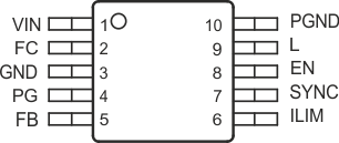
6 Pin Configuration and Functions
DGS Package
10-Pin VSSOP
Top View

Pin Functions
| PIN | I/O | DESCRIPTION | |
|---|---|---|---|
| NAME | NO. | ||
| EN | 8 | I | Enable. A logic high enables the converter, logic low forces the device into shutdown mode reducing the supply current to less than 1 μA. |
| FB | 5 | I | Feedback pin for the fixed output voltage option. For the adjustable version an external resistive divider is connected to FB. The internal voltage divider is disabled for the adjustable version. |
| FC | 2 | — | Supply bypass pin. A 0.1-μF coupling capacitor should be connected as close as possible to this pin for good high frequency input voltage supply filtering. |
| GND | 3 | — | Ground |
| ILIM | 6 | I | Switch current limit. Connect ILIM to GND to set the switch current limit to typically 600 mA, or connect this pin to VIN to set the current limit to typically 1200 mA. |
| L | 9 | I/O | Connect the inductor to this pin. L is the switch pin connected to the drain of the internal power MOSFETS. |
| PG | 4 | O | Power good comparator output. This is an open-drain output. A pull-up resistor should be connected between PG and VOUT. The output goes active high when the output voltage is greater than 92% of the nominal value. |
| PGND | 10 | — | Power ground. Connect all power grounds to PGND. |
| SYNC | 7 | I | Input for synchronization to external clock signal. Synchronizes the converter switching frequency to an external clock signal with CMOS level: SYNC = High: Low-noise mode enabled, fixed frequency PWM operation is forced SYNC = Low (GND): Power save mode enabled, PFM/PWM mode enabled |
| VIN | 1 | I | Supply voltage input |