SLVS432F September 2002 – June 2015 TPS62050 , TPS62051 , TPS62052 , TPS62054 , TPS62056
PRODUCTION DATA.
- 1 Features
- 2 Applications
- 3 Description
- 4 Typical Application Schematic
- 5 Revision History
- 6 Device Comparison Table
- 7 Pin Configuration and Functions
- 8 Specifications
- 9 Detailed Description
- 10Application and Implementation
- 11Power Supply Recommendations
- 12Layout
- 13Device and Documentation Support
- 14Mechanical, Packaging, and Orderable Information
パッケージ・オプション
デバイスごとのパッケージ図は、PDF版データシートをご参照ください。
メカニカル・データ(パッケージ|ピン)
- DGS|10
サーマルパッド・メカニカル・データ
発注情報
1 Features
- High-Efficiency Synchronous Step-Down
Converter With up to 95% Efficiency - 12-µA Quiescent Current (Typical)
- 2.7-V to 10-V Operating Input Voltage Range
- Adjustable Output Voltage Range: 0.7 V to 6 V
- Fixed Output Voltage Options Available With
1.5 V, 1.8 V, and 3.3 V - Synchronizable to External Clock: Up to 1.2 MHz
- High-Efficiency Over a Wide Load Current Range in Power-Save Mode
- 100% Maximum Duty Cycle for Lowest Dropout
- Low-Noise Operation in Forced Fixed-
Frequency PWM Operation Mode - Internal Softstart
- Overtemperature and Overcurrent Protected
- Available in 10-Pin Micro-Small Outline
Package MSOP
2 Applications
- Cellular Phones
- Organizers, PDAs, and Handheld PCs
- Low-Power DSP Supplies
- Digital Cameras and Hard Disks
3 Description
The TPS6205x devices are a family of high-efficiency synchronous step-down DC-DC converters that are ideally suited for systems powered from a 1- or 2-cell Li-Ion battery or from a 3- to 5-cell NiCd, NiMH, or alkaline battery.
The TPS6205x devices are synchronous pulse width modulation (PWM) converters with integrated N- and P-channel power MOSFET switches. Synchronous rectification increases efficiency and reduces external component count. To achieve highest efficiency over a wide load current range, the converter enters a power-saving pulse frequency modulation (PFM) mode at light load currents. Operating frequency is typically 850 kHz, allowing the use of small inductor and capacitor values. The device can be synchronized to an external clock signal in the range of 600 kHz to 1.2 MHz. For low noise operation, the converter can be programmed into forced-fixed frequency in PWM mode. In shutdown mode, the current consumption is reduced to less than 2 µA. The TPS6205x devices are available in the 10-pin (DGS) micro-small outline package (MSOP) and operates over a free air temperature range of –40°C to 85°C.
Device Information(1)
| PART NUMBER | PACKAGE | BODY SIZE (NOM) |
|---|---|---|
| TPS62050 | VSSOP (10) | 3.00 mm × 3.00 mm |
| TPS62051 | ||
| TPS62052 | ||
| TPS62054 | ||
| TPS62056 |
- For all available packages, see the orderable addendum at the end of the data sheet.
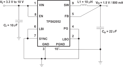
4 Typical Application Schematic

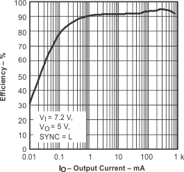
Efficiency vs Output Current
