SLVS833E March   2010  – October 2020 TPS62065 , TPS62067

PRODUCTION DATA  

  1. Features
  2. Applications
  3. Description
  4. Revision History
  5. Device Comparison Table
  6. Pin Configuration and Functions
  7. Specifications
    1. 7.1 Absolute Maximum Ratings
    2. 7.2 ESD Ratings
    3. 7.3 Recommended Operating Conditions
    4. 7.4 Thermal Information
    5. 7.5 Electrical Characteristics
    6. 7.6 Typical Characteristics
  8. Detailed Description
    1. 8.1 Overview
    2. 8.2 Functional Block Diagram
    3. 8.3 Feature Description
      1. 8.3.1 Mode Selection (TPS62065)
      2. 8.3.2 Power Good Output (TPS62067)
      3. 8.3.3 Enable
      4. 8.3.4 Clock Dithering
      5. 8.3.5 Undervoltage Lockout
      6. 8.3.6 Thermal Shutdown
    4. 8.4 Device Functional Modes
      1. 8.4.1 Soft Start
      2. 8.4.2 Power Save Mode
      3. 8.4.3 Dynamic Voltage Positioning
      4. 8.4.4 100% Duty Cycle Low Dropout Operation
      5. 8.4.5 Internal Current Limit and Fold-Back Current Limit for Short Circuit Protection
      6. 8.4.6 Output Capacitor Discharge
  9. Application and Implementation
    1. 9.1 Application Information
    2. 9.2 Typical Application
      1. 9.2.1 Design Requirements
      2. 9.2.2 Detailed Design Procedure
        1. 9.2.2.1 Output Voltage Setting
        2. 9.2.2.2 Output Filter Design (Inductor and Output Capacitor)
          1. 9.2.2.2.1 Inductor Selection
          2. 9.2.2.2.2 Output Capacitor Selection
          3. 9.2.2.2.3 Input Capacitor Selection
        3. 9.2.2.3 Checking Loop Stability
      3. 9.2.3 Application Curves
    3. 9.3 System Example
      1. 9.3.1 TPS62067 Adjustable 1.8-V Output
  10. 10Power Supply Recommendations
  11. 11Layout
    1. 11.1 Layout Guidelines
    2. 11.2 Layout Example
  12. 12Device and Documentation Support
    1. 12.1 Device Support
      1. 12.1.1 Third-Party Products Disclaimer
    2. 12.2 Related Links
    3. 12.3 Receiving Notification of Documentation Updates
    4. 12.4 Support Resources
    5. 12.5 Trademarks
    6. 12.6 Electrostatic Discharge Caution
    7. 12.7 Glossary
  13. 13Mechanical, Packaging, and Orderable Information

パッケージ・オプション

メカニカル・データ(パッケージ|ピン)
サーマルパッド・メカニカル・データ
発注情報

Description

The TPS6206x is a family of highly efficient synchronous step down DC/DC converters. They provide up to 2-A output current.

With an input voltage range of 2.9 V to 6 V, the device is a perfect fit for power conversion from a 5-V or 3.3-V system supply rail. The TPS6206x operates at 3-MHz fixed frequency and enters power save mode operation at light load currents to maintain high efficiency over the entire load current range. The power save mode is optimized for low output voltage ripple. For low noise applications, TPS62065 can be forced into fixed frequency PWM mode by pulling the MODE pin high. TPS62067 provides an open drain power good output.

In the shutdown mode, the current consumption is reduced to less than 1 µA and an internal circuit discharges the output capacitor.

TPS6206x family is optimized for operation with a tiny 1 µH inductor and a small 10-µF output capacitor to achieve smallest solution size and high regulation performance.

It is available in a small 2-mm × 2-mm × 0.75-mm 8-pin WSON package.

Device Information
PART NUMBERPACKAGE(1)BODY SIZE (NOM)
TPS62065
TPS62067
WSON (8)2.00 mm × 2.00 mm
For all available packages, see the orderable addendum at the end of the data sheet.
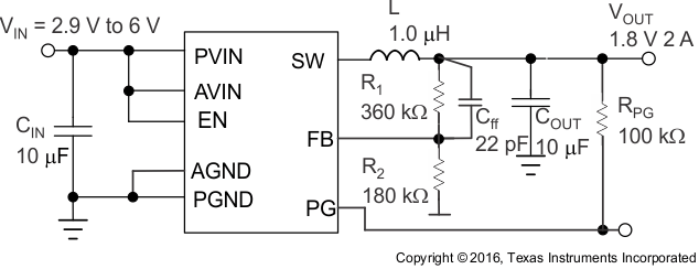
GUID-D7F83302-212F-45BB-B534-AE8F647B8503-low.gifTypical Application Schematic
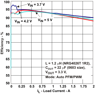
GUID-69C095AF-7795-4D27-923F-1AC9C8D335F5-low.gifEfficiency vs Load Current