JAJSE91A September 2017 – December 2017 TPS62097-Q1
PRODUCTION DATA.
- 1 特長
- 2 アプリケーション
- 3 概要
- 4 改訂履歴
- 5 Terminal Configuration and Functions
- 6 Specifications
- 7 Detailed Description
- 8 Application Information
- 9 Power Supply Recommendations
- 10PCB Layout
- 11デバイスおよびドキュメントのサポート
- 12メカニカル、パッケージ、および注文情報
パッケージ・オプション
デバイスごとのパッケージ図は、PDF版データシートをご参照ください。
メカニカル・データ(パッケージ|ピン)
- RGT|16
サーマルパッド・メカニカル・データ
発注情報
6 Specifications
6.1 Absolute Maximum Ratings(1)
| MIN | MAX | UNIT | ||
|---|---|---|---|---|
| Voltage at Pins(2) | AVIN, PVIN, EN, VOS, PG | –0.3 | 6.0 | V |
| MODE, SS/TR, SW (DC) | –0.3 | VIN+0.3V | ||
| FB | –0.3 | 3.0 | ||
| SW (AC, less than 100ns)(3) | -3 | 11 | ||
| Sink current | PG | 0 | 1.0 | mA |
| Temperature | Operating Junction, TJ | -40 | 150 | °C |
| Storage, Tstg | –65 | 150 |
(1) Stresses beyond those listed under absolute maximum ratings may cause permanent damage to the device. These are stress ratings only, and functional operation of the device at these or any other conditions beyond those indicated under recommended operating conditions is not implied. Exposure to absolute-maximum-rated conditions for extended periods may affect device reliability.
(2) All voltage values are with respect to network ground terminal.
(3) While switching.
6.2 ESD Ratings
| VALUE | UNIT | ||||
|---|---|---|---|---|---|
| VESD | Electrostatic discharge | Human-body model (HBM), per AEC Q100-002(1) | ±2500 | V | |
| Charged-device model (CDM), per AEC Q100-011(1) | ±1500 | ||||
(1) AEC Q100-002 indicates that HBM stressing shall be in accordance with the ANSI/ESDA/JEDEC JS-001 specification.
6.3 Recommend Operating Conditions
| MIN | MAX | UNIT | ||
|---|---|---|---|---|
| VIN | Input voltage range | 2.5 | 6.0 | V |
| VPG | Pull-up resistor voltage | 0 | 6.0 | V |
| VOUT | Output voltage range | 0.8 | VIN | V |
| IOUT | Output current range | 0 | 2.0 | A |
| TJ | Operating junction temperature | -40 | 125 | °C |
6.4 Thermal Information
| THERMAL METRIC(1) | TPS62097-Q1WRGT | UNITS | |
|---|---|---|---|
| RθJA | Junction-to-ambient thermal resistance | 44.2 | °C/W |
| RθJC(top) | Junction-to-case (top) thermal resistance | 51.7 | °C/W |
| RθJB | Junction-to-board thermal resistance | 19.3 | °C/W |
| ψJT | Junction-to-top characterization parameter | 1.1 | °C/W |
| ψJB | Junction-to-board characterization parameter | 19.3 | °C/W |
| RθJC(bot) | Junction-to-case (bottom) thermal resistance | 3.6 | °C/W |
(1) For more information about traditional and new thermal metrics, see the IC Package Thermal Metrics application report, SPRA953
6.5 Electrical Characteristics
TJ = -40°C to 125°C, and VIN = 2.5V to 6.0V. Typical values are at TJ = 25°C and VIN = 3.6V, unless otherwise noted.| PARAMETER | TEST CONDITIONS | MIN | TYP | MAX | UNIT | |
|---|---|---|---|---|---|---|
| SUPPLY | ||||||
| IQ | Quiescent current into AVIN, PVIN | EN = High, Device not switching, TJ = –40°C to 85°C | 40 | 57 | µA | |
| EN = High, Device not switching | 40 | 65 | ||||
| ISD | Shutdown current into AVIN, PVIN | EN = Low, TJ = –40°C to 85°C | 0.7 | 3 | µA | |
| EN = Low | 0.7 | 10 | ||||
| VUVLO | Under voltage lock out threshold | VIN falling | 2.2 | 2.3 | 2.4 | V |
| VIN rising | 2.3 | 2.4 | 2.5 | |||
| TQ JSD | Thermal shutdown threshold | TJ rising | 160 | °C | ||
| Thermal shutdown hysteresis | TJ falling | 20 | °C | |||
| LOGIC INTERFACE (EN, MODE) | ||||||
| VH_EN | High-level input voltage, EN pin | 1.6 | 2.0 | V | ||
| VL_EN | Low-level input voltage, EN pin | 1.0 | 1.3 | V | ||
| IEN,LKG | Input leakage current into EN pin | EN = High | 0.01 | 0.9 | µA | |
| RPD | Pull-down resistance at EN pin | EN = Low | 375 | kΩ | ||
| VH_MO | High-level input voltage, MODE pin | 1.2 | V | |||
| VL_MO | Low-level input voltage, MODE pin | 0.4 | V | |||
| IMO,LKG | Input leakage current into MODE pin | MODE = High | 0.01 | 0.16 | µA | |
| SOFT STARTUP, POWER GOOD (SS/TR, PG) | ||||||
| ISS | Soft startup current | 5.5 | 7.5 | 9.5 | µA | |
| Voltage tracking gain factor | VFB / VSS/TR | 1 | ||||
| VPG | Power good threshold | VOUT rising, referenced to VOUT nominal | 92 | 95 | 98 | % |
| VOUT falling, referenced to VOUT nominal | 87 | 90 | 92 | |||
| VPG,OL | Low-level output voltage, PG pin | Isink = 1mA | 0.4 | V | ||
| IPG,LKG | Input leakage current into PG pin | VPG = 5.0V | 0.01 | 1.6 | µA | |
| OUTPUT | ||||||
| VOUT | Output voltage accuracy TPS6209733Q |
PWM mode, No load | –1.0 | 1.0 | % | |
| PSM mode(1) | –1.0 | 2.1 | ||||
| VFB | Feedback reference voltage | PWM mode | 792 | 800 | 808 | mV |
| PSM mode(1) | 792 | 800 | 817 | |||
| IFB,LKG | Input leakage current into FB pin | VFB = 0.8V | 0.01 | 0.1 | µA | |
| RDIS | Output discharge resistor | EN = Low, VOUT = 1.8V | 165 | Ω | ||
| Line regulation | IOUT = 0.5A, VOUT = 1.8V(1) | 0.02 | %/V | |||
| Load regulation | PWM mode, VOUT = 1.8V (1) | 0.2 | %/A | |||
| POWER SWITCH | ||||||
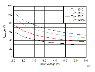
| RDS(on) | High-side FET on-resistance | ISW = 500mA, VIN = 5.0V | 42 | mΩ | ||
| ISW = 500mA, VIN = 3.6V | 53 | |||||
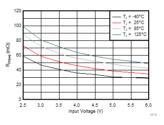
| Low-side FET on-resistance | ISW = 500mA, VIN = 5.0V | 40 | mΩ | |||
| ISW = 500mA, VIN = 3.6V | 50 | |||||
| ILIMF | High-side FET forward current limit | 3.1 | 3.6 | 4.2 | A | |
| VIN = 5.0V | 3.3 | 3.6 | 3.9 | |||
| ILIMN | Low-side FET negative current limit | Forced PWM mode | –1.25 | –1.1 | -0.7 | A |
(1) Conditions: L = 1μH, COUT = 22μF, Switching Frequency = 2.0MHz
6.6 Typical Characteristics
 Figure 1. High-Side FET On-Resistance
 Figure 2. Low-Side FET On-Resistance