VIN = 12 V, VOUT = 3.3 V, TA = 25°C, (unless otherwise noted)
VIN = 12 V, VOUT = 3.3 V, TA = 25°C, (unless otherwise noted) 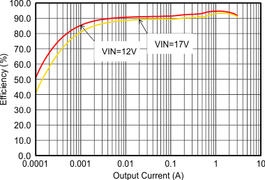 Figure 9-4 Efficiency with 1.25 MHz. VIN = 12 V, VOUT = 3.3 V, TA = 25°C, (unless otherwise noted)
 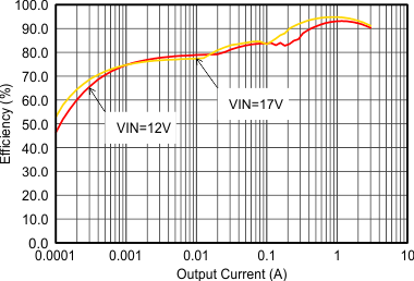 Figure 9-6 Efficiency with 2.5 MHz
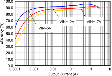 Figure 9-8 Efficiency with 1.25 MHz
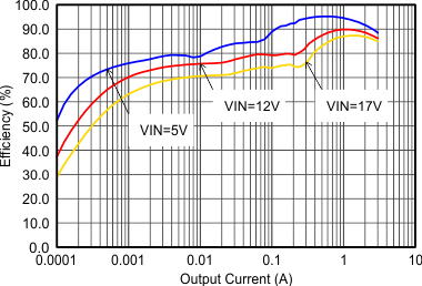 Figure 9-10 Efficiency with 2.5 MHz
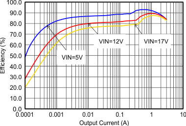 Figure 9-12 Efficiency with 1.25 MHz
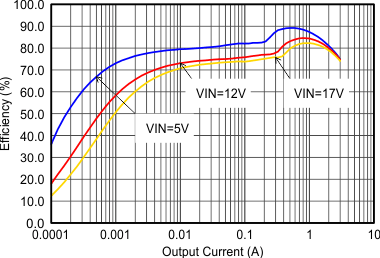 Figure 9-14 Efficiency with 1.25 MHz
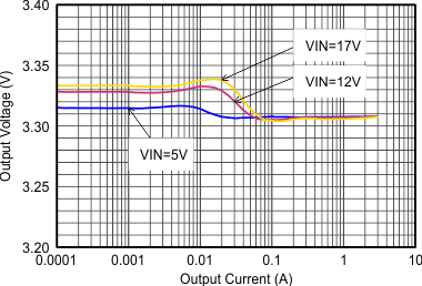 Figure 9-16 Output Voltage Accuracy (Load Regulation)
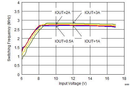 Figure 9-18 Switching Frequency vs Input Voltage
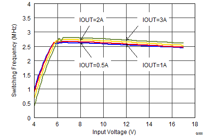 Figure 9-20 Switching Frequency vs Input Voltage
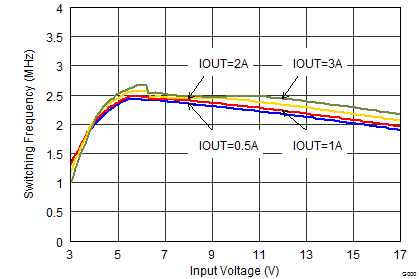 Figure 9-22 Switching Frequency vs Input Voltage
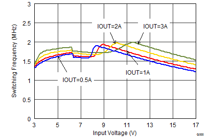 Figure 9-24 Switching Frequency vs Input Voltage
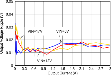 Figure 9-26 Output Voltage Ripple
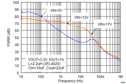 Figure 9-28 Power Supply Rejection Ratio
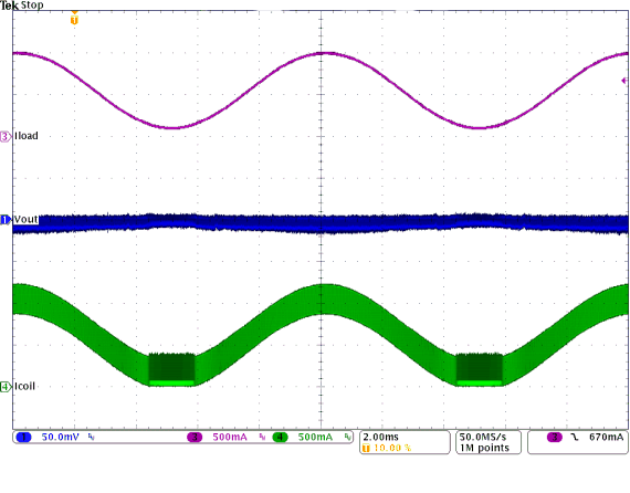
| VIN = 12 | VOUT = 3.3 V with 50 mV/Div |
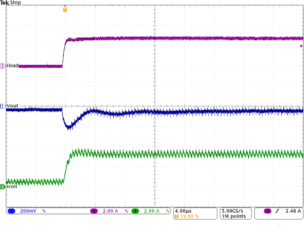 Figure 9-32 Load Transient Response of Figure 9-31, Rising Edge
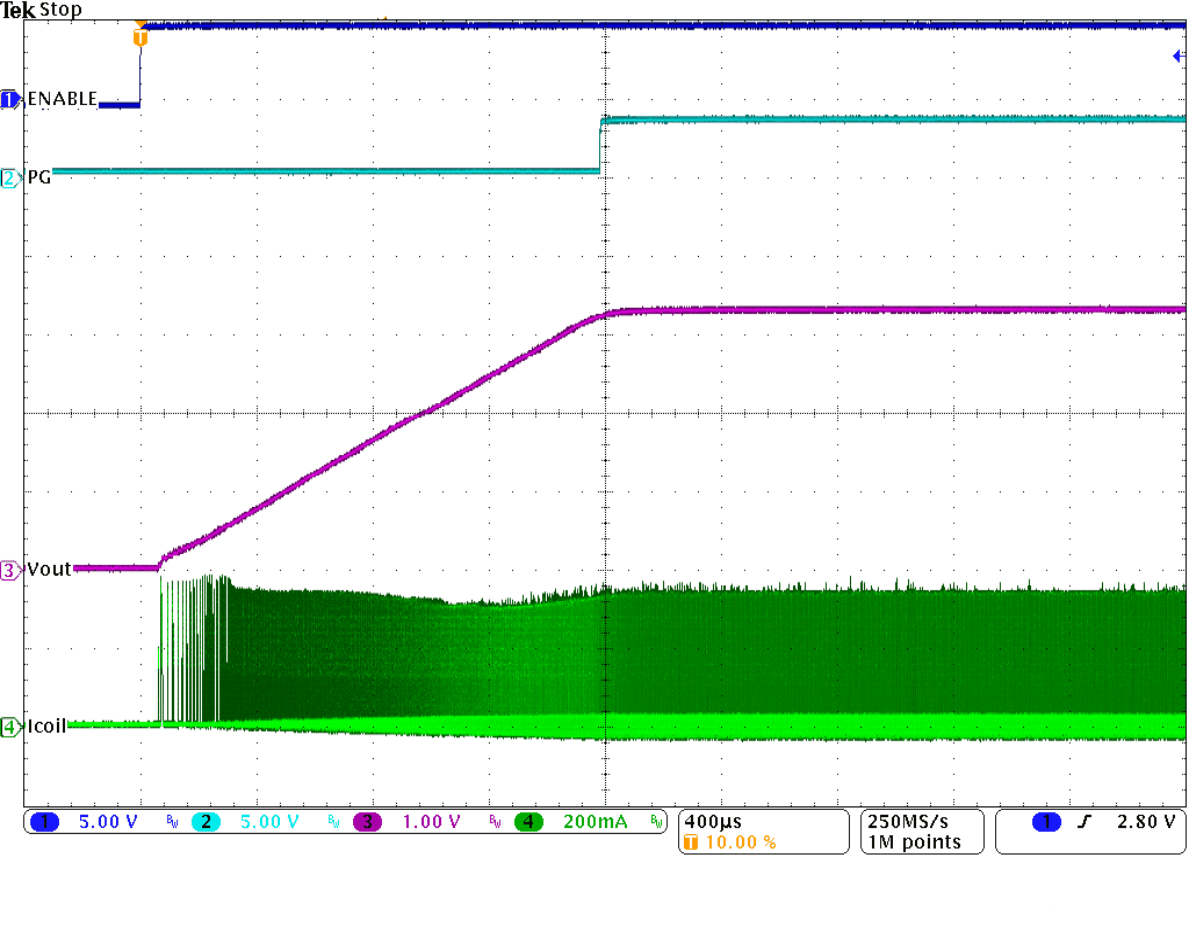 Figure 9-34 Start-Up Into 100
mA
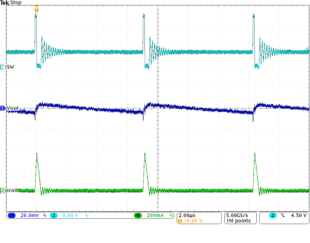
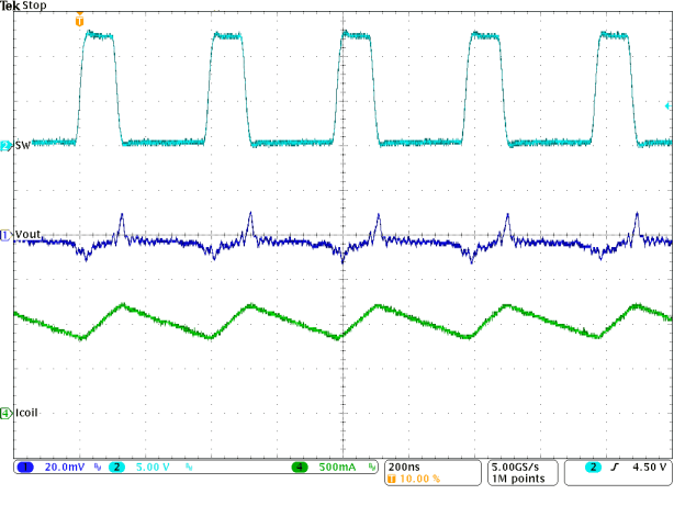 Figure 9-36 Typical Operation In PWM Mode
| FSW = 2.5 MHz | | TPS62130EVM |
| L = 2.2 µH (XFL4020) |
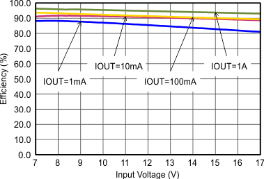 Figure 9-5 Efficiency with 1.25 MHz
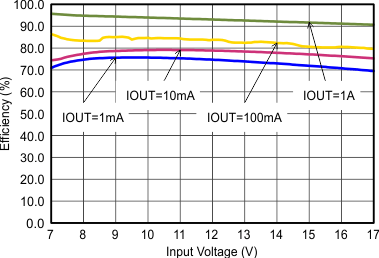 Figure 9-7 Efficiency with 2.5 MHz
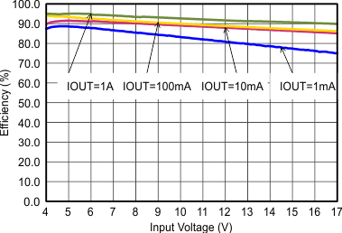 Figure 9-9 Efficiency with 1.25 MHz
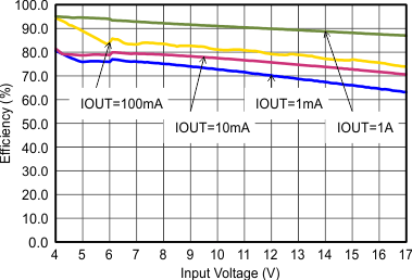 Figure 9-11 Efficiency with 2.5 MHz
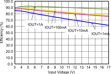 Figure 9-13 Efficiency with 1.25 MHz
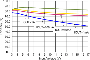 Figure 9-15 Efficiency with 1.25 MHz
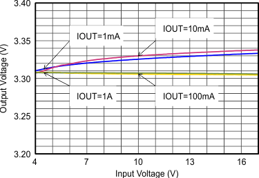 Figure 9-17 Output Voltage Accuracy (Line Regulation)
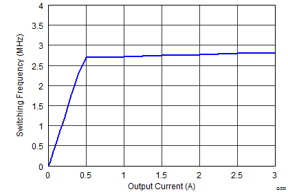 Figure 9-19 Switching Frequency vs Output Current
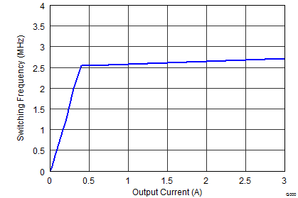 Figure 9-21 Switching Frequency vs Output Current,
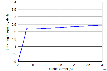 Figure 9-23 Switching Frequency vs Output Current
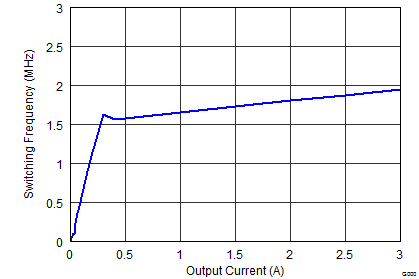 Figure 9-25 Switching Frequency vs Output Current
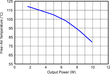
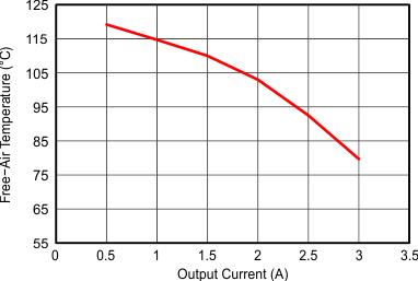
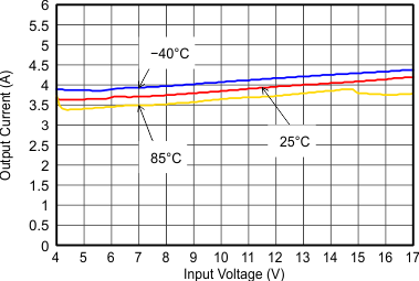 Figure 9-27 Maximum Output Current
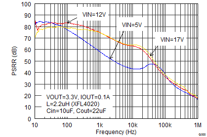 Figure 9-29 Power Supply Rejection Ratio
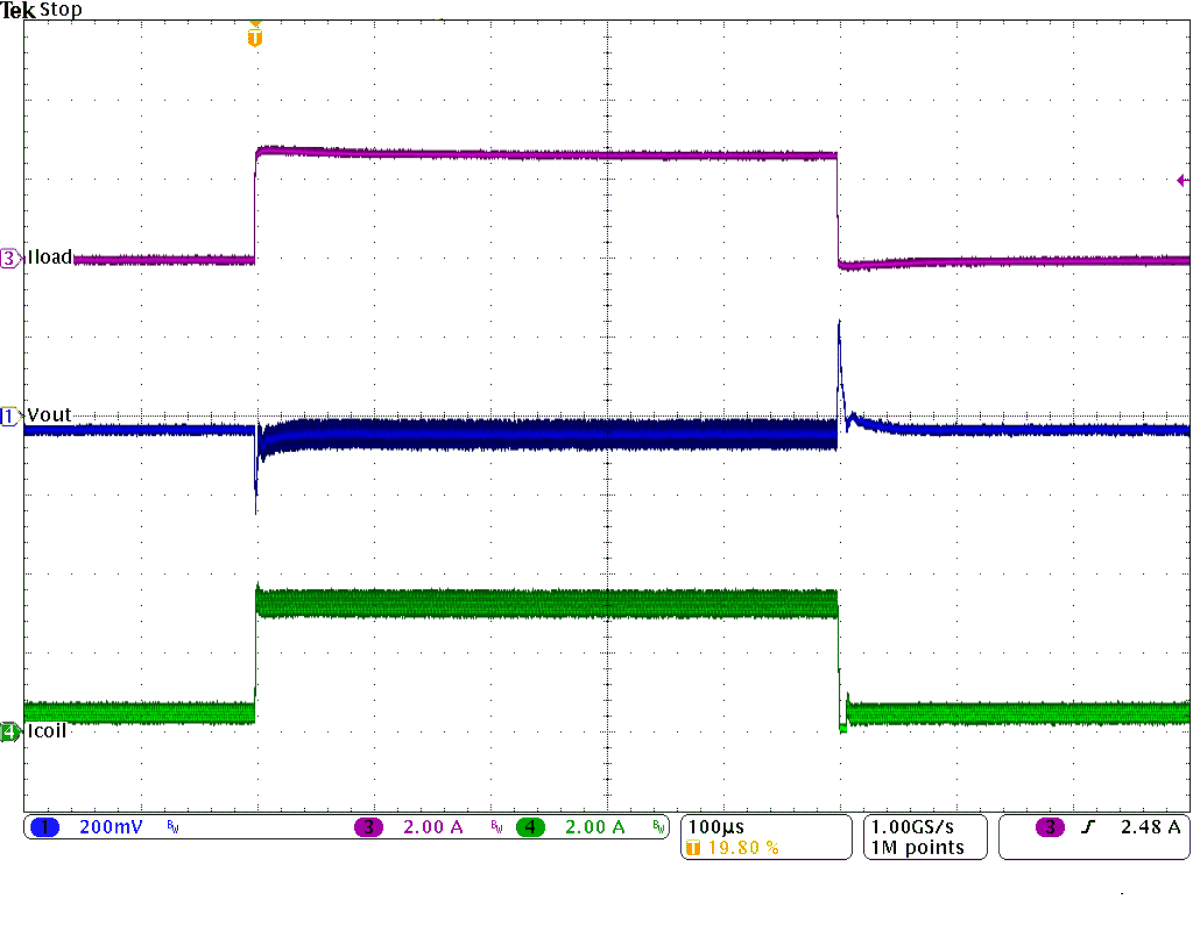 Figure 9-31 Load Transient Response
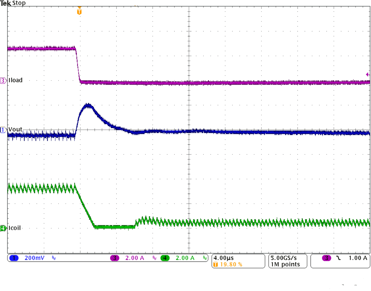 Figure 9-33 Load Transient Response of Figure 9-31, Falling Edge
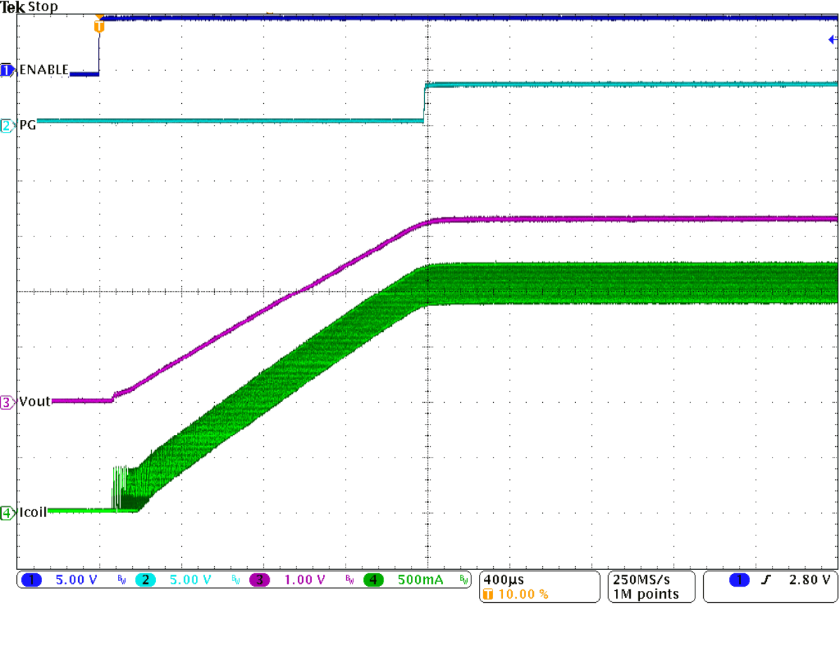 Figure 9-35 Start-Up Into 3 A
 Figure 9-37 Typical Operation In Power Save Mode
| FSW = 2.5 MHz | | TPS62130EVM |
| L = 2.2 µH (XFL4020) |


 Figure 9-16 Output Voltage Accuracy (Load Regulation)


 Figure 9-26 Output Voltage Ripple

 Figure 9-32 Load Transient Response of Figure 9-31, Rising Edge
 Figure 9-34 Start-Up Into 100
mA


 Figure 9-17 Output Voltage Accuracy (Line Regulation)


 Figure 9-27 Maximum Output Current

 Figure 9-33 Load Transient Response of Figure 9-31, Falling Edge
 Figure 9-35 Start-Up Into 3 A