SLVSC20E January 2015 – October 2016 TPS62134A , TPS62134B , TPS62134C , TPS62134D
PRODUCTION DATA.
- 1 Features
- 2 Applications
- 3 Description
- 4 Revision History
- 5 Device Comparison Table
- 6 Pin Configuration and Functions
- 7 Specifications
-
8 Detailed Description
- 8.1 Overview
- 8.2 Functional Block Diagram
- 8.3
Feature Description
- 8.3.1 Enable and Shutdown (EN)
- 8.3.2 Undervoltage Lockout (UVLO)
- 8.3.3 Soft-Start (SS) Circuitry
- 8.3.4 Switch Current-Limit and Short Circuit Protection
- 8.3.5 Output Voltage and LPM Logic Selection (VIDx and LPM)
- 8.3.6 Power-Good Output (PG)
- 8.3.7 Single-Ended Remote Sense (FBS)
- 8.3.8 Thermal Shutdown
- 8.4 Device Functional Modes
- 9 Application and Implementation
- 10Power Supply Recommendations
- 11Layout
- 12Device and Documentation Support
- 13Mechanical, Packaging, and Orderable Information
パッケージ・オプション
メカニカル・データ(パッケージ|ピン)
- RGT|16
サーマルパッド・メカニカル・データ
- RGT|16
発注情報
8 Detailed Description
8.1 Overview
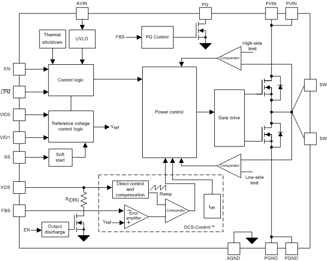
The TPS62134x synchronous switched-mode power converters are based on DCS-Control™ (direct control with seamless transition into power-save mode), an advanced regulation topology that combines the advantages of hysteretic, voltage-mode, and current-mode control including an AC loop that is directly associated to the output voltage. This control loop uses information about output voltage changes and feeds the information directly to a fast comparator stage. The control loop provides immediate response to dynamic load changes. For accurate DC load regulation, a voltage feedback loop is used. The internally compensated regulation network achieves fast and stable operation with small external components and low ESR capacitors.
The DCS-Control™ topology supports PWM (pulse width modulation) mode for medium and heavy load conditions and a power-save mode (PSM) at light loads. During PWM mode, the devices operate at the nominal switching frequency in continuous conduction mode (CCM). This frequency is approximately 1 MHz (typical) with a controlled frequency variation depending on the input voltage. If the load current decreases, the converter enters PSM to sustain high efficiency down to very light loads. In PSM, the switching frequency decreases linearly with the load current. Because DCS-Control™ supports both operation modes within one single building block, the transition from PWM to PSM is seamless without effects on the output voltage.
8.3 Feature Description
8.3.1 Enable and Shutdown (EN)
When the EN pin is set high, the device begins operation. The EN pin allows sequencing from a host or power-good output of another device.
The devices enter shutdown mode if the EN pin is pulled low with a shutdown current of 2 µA (typical). During shutdown, the internal power MOSFETs as well as the entire control circuitry are turned off. The output capacitor is smoothly discharged by a 20-kΩ internal resistor through the VOS pin. An internal pulldown resistor of approximately 400 kΩ is connected and maintains EN logic low, if the pin is floating. The pulldown resistor is disconnected if the EN pin is high.
8.3.2 Undervoltage Lockout (UVLO)
If the input voltage drops, the undervoltage lockout prevents misoperation of the device by switching off both power MOSFETs. The UVLO threshold is set to 2.7 V (typical). The device is fully operational for voltages above the UVLO threshold and turns off if the input voltage trips the threshold. The converter begins operation again when the input voltage exceeds the threshold by a hysteresis of 200 mV (typical).
8.3.3 Soft-Start (SS) Circuitry
The internal soft-start circuitry controls the output-voltage slope during startup. This control avoids excessive inrush current and ensures a controlled output-voltage rise time. The control also prevents unwanted voltage drops from high-impedance power sources or batteries. When the EN pin is set high to begin device operation, the device begins switching after a delay of approximately 50 µs and VO rises up to the nominal value set by the VIDx pins with a slope controlled by an external capacitor connected to the SS pin. Leave the SS pin floating for the fastest startup.
The device can startup into a pre-biased output. During monotonic pre-biased startup, both power MOSFETs are not allowed to turn on until the internal ramp of the device sets an output voltage above the pre-bias voltage.
If the device is in shutdown mode, undervoltage lockout, or thermal shutdown, an internal resistor pulls the SS pin down to ensure a proper low level. Returning from those states causes a new startup sequence.
8.3.4 Switch Current-Limit and Short Circuit Protection
The TPS62134x family of devices is protected against heavy load and short circuit events. If an output short circuit is detected (VO drops below 0.3 V), the switch current limit is reduced to 1.6 A (typical). If the output voltage rises above 0.4 V, the device operates in normal operation again.
At heavy loads, the current-limit determines the maximum output current. The current-limit supports output currents of 3 A with input voltages below 5 V and 3.2 A with higher input voltages. If the peak current-limit (IL) is reached, the high-side MOSFET is turned off. Avoiding shoot-through current, the low-side MOSFET is switched on to sink the inductor current. The high-side MOSFET turns on again, only if the current in the low-side MOSFET has decreased below the low-side current-limit threshold of 3.2 A (typical).
Because of the internal propagation delay, the actual peak current of the high-side switch typically occurs above the DC value listed in the Electrical Characteristic table, especially in low duty-cycle applications. Use Equation 1 to calculate the dynamic current-limit.

8.3.5 Output Voltage and LPM Logic Selection (VIDx and LPM)
The output voltage of the TPS62134x family of devices is selected by two VIDx pins and one LPM pin as listed in Table 1. A pulldown resistor of 400 kΩ is internally connected to the VIDx pins and LPM pin to ensure a proper logic level if the pin is high impedance or floating. The pulldown resistors are disconnected if the pins are pulled High.
The device has a low power mode (LPM) where the output voltage is reduced or disabled by using the LPM pin. While the LPM pin is asserted, the PG output remains high impedance. The device also achieves a dynamic output-voltage change by using the VIDx pins. This feature helps the system to minimize power consumption in standby or idle mode. The TPS62134B/D devices provide the full current even if the output voltage is set at 0.7 V in LPM mode.
Table 1. Output Voltage Selection
| PART NUMBER (INTEL SKYLAKE VRs) |
LPM LOGIC | VID1 LOGIC | VID0 LOGIC | OUTPUT VOLTAGE (V) |
|---|---|---|---|---|
| TPS62134A (VCC(IO) Rail) |
0 | x | x | 0 (LPM) |
| 1 | 0 | 0 | 0.850 | |
| 1 | 0 | 1 | 0.875 | |
| 1 | 1 | 0 | 0.950 | |
| 1 | 1 | 1 | 0.975 | |
| TPS62134B (VCC(PRIM_CORE) Rail) |
0 | x | x | 0.7 (LPM) |
| 1 | 0 | 0 | 0.80 | |
| 1 | 0 | 1 | 0.85 | |
| 1 | 1 | 0 | 0.90 | |
| 1 | 1 | 1 | 0.95 | |
| TPS62134C (VCC(EDRAM) / VCC(EOPIO) Rail) |
0 | x | x | 0 (LPM) |
| 1 | 0 | 0 | 0.80 | |
| 1 | 0 | 1 | 0.95 | |
| 1 | 1 | 0 | 1.00 | |
| 1 | 1 | 1 | 1.05 | |
| TPS62134D (VCC(PRIM_CORE) Rail) |
0 | x | x | 0.7 (LPM) |
| 1 | 0 | 0 | 0.85 | |
| 1 | 0 | 1 | 0.90 | |
| 1 | 1 | 0 | 0.95 | |
| 1 | 1 | 1 | 1.00 |
8.3.6 Power-Good Output (PG)
The TPS62134x family of devices has a built-in power-good indicator. The PG signal can be used for startup sequencing of multiple rails. The PG pin is an open-drain output that requires a pullup resistor to any voltage below 6 V. The device has a fixed power-good threshold of 760 mV (rising edge) and 720 mV (falling edge). The PG rising edge has a delay time of 140 µs (typical) and a falling edge has a delay time of 20 µs (typical). The PG pin can sink 2-mA of current and maintain the specified logic low level. Table 2 lists the PG logic status in different operation conditions. The PG pin can be left floating if not used.
In LPM, the PG signal is latched as high impedance. When the device exits LPM, the PG has a 500-µs blanking time to ensure that the output voltage returns to the nominal value.
NOTE
For the TPS62134A and TPS62134C, if LPM is exited when the output voltage is between 0.5 V to 0.75 V, the PG pin may not have its 500-µs blanking time and may go briefly low as the output voltage returns to its set-point. To avoid this behavior, do not enter LPM or adjust the load and/or output capacitance or add an extra output discharge circuit to avoid this output voltage range when LPM is exited.
The TPS62134A and TPS62134C are not recommended for new Skylake or KabyLake, Intel designs. The TPS62134B or TPS62134D should be used in their place. These parts are pin to pin compatible facilitating a simple replacement. See Table 1 for VID related changes.
Table 2. Power Good Logic
| CONDITIONS | PG LOGIC STATUS | ||
|---|---|---|---|
| HIGH IMPEDANCE | LOW | ||
| Enable | EN = high, LPM = high, VO > 760 mV | √ | |
| EN = high, LPM = high, VO < 720 mV | √ | ||
| LPM | EN = high, LPM = low | √ | |
| LPM, TPS62134B/D | EN = high, LPM = Low, VO < 0.3 V | √ | |
| Shutdown | EN = Low | √ | |
| Thermal shutdown | √ | ||
| UVLO | 0.5 V < V(AVIN) < V(UVLO) | √ | |
| Power supply removal | V(AVIN) < 0.5 V | √ | |
8.3.7 Single-Ended Remote Sense (FBS)
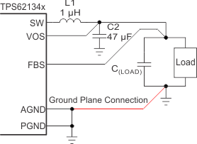
The devices allow a single-ended remote sense by connecting the FBS pin at the load. This function overcomes the parasitic resistance of the PCB traces and achieves an improved output-voltage regulation at the load. Avoid any noise coupled into the FBS trace. Use a solid ground plane to connect the ground return of the load with the AGND and PGND pins of the device. Connect the AGND and PGND pins directly to exposed thermal pad of the device. Figure 3 shows an example.
 Figure 3. Remote Sense Connection
8.3.8 Thermal Shutdown
The junction temperature (TJ) of the device is monitored by an internal temperature sensor. If TJ exceeds 160°C (typical), the device goes into thermal shutdown. Both the high-side and low-side power MOSFETs are turned off. When TJ decreases below the hysteresis of 20°C, the converter resumes normal operation, beginning with a soft start.
8.4 Device Functional Modes
8.4.1 PWM Operation and Power Save Mode
The device operates with pulse width modulation (PWM) in medium and heavy load with a fixed on-time circuitry (ton). Use Equation 2 to calculate the on-time in steady-state operation.

The typical PWM switching frequency is 1 MHz. The frequency variation in PWM is controlled and depends on VI, VO, and the inductance. The switching frequency decreases with the input voltage to improve the efficiency in small duty-cycle applications.
To maintain high efficiency at light loads, the device enters PSM at the boundary to discontinuous conduction mode (DCM). In PSM, the switching frequency decreases linearly with the load current maintaining high efficiency. Use Equation 3 to calculate the switching frequency in PSM mode.

See Figure 12 for the switching frequency variation over load and input voltage.
